Microfluidic Fabrication Techniques for High-Pressure Testing of Microscale Supercritical CO2 Foam Transport in Fractured Unconventional Reservoirs
Summary
This paper describes a protocol along with a comparative study of two microfluidic fabrication techniques, namely photolithography/wet-etching/thermal-bonding and Selective Laser-induced Etching (SLE), that are suitable for high-pressure conditions. These techniques constitute enabling platforms for direct observation of fluid flow in surrogate permeable media and fractured systems under reservoir conditions.
Abstract
Pressure limitations of many microfluidic platforms have been a significant challenge in microfluidic experimental studies of fractured media. As a result, these platforms have not been fully exploited for direct observation of high-pressure transport in fractures. This work introduces microfluidic platforms that enable direct observation of multiphase flow in devices featuring surrogate permeable media and fractured systems. Such platforms provide a pathway to address important and timely questions such as those related to CO2 capture, utilization and storage. This work provides a detailed description of the fabrication techniques and an experimental setup that may serve to analyze the behavior of supercritical CO2 (scCO2) foam, its structure and stability. Such studies provide important insights regarding enhanced oil recovery processes and the role of hydraulic fractures in resource recovery from unconventional reservoirs. This work presents a comparative study of microfluidic devices developed using two different techniques: photolithography/wet-etching/thermal-bonding versus Selective Laser-induced Etching. Both techniques result in devices that are chemically and physically resistant and tolerant of high pressure and temperature conditions that correspond to subsurface systems of interest. Both techniques provide pathways to high-precision etched microchannels and capable lab-on-chip devices. Photolithography/wet-etching, however, enables fabrication of complex channel networks with complex geometries, which would be a challenging task for laser etching techniques. This work summarizes a step-by-step photolithography, wet-etching and glass thermal-bonding protocol and, presents representative observations of foam transport with relevance to oil recovery from unconventional tight and shale formations. Finally, this work describes the use of a high-resolution monochromatic sensor to observe scCO2 foam behavior where the entirety of the permeable medium is observed simultaneously while preserving the resolution needed to resolve features as small as 10 µm.
Introduction
Hydraulic fracturing has been used for quite some time as a means to stimulate flow especially in tight formations1. Large amounts of water needed in hydraulic fracturing are compounded with environmental factors, water-availability issues2, formation damage3, cost4 and seismic effects5. As a result, interest in alternate fracturing methods such as waterless fracturing and the use of foams is on the rise. Alternative methods may provide important benefits such as reduction in water use6, compatibility with water sensitive formations7, minimal to no plugging of the formation8, high apparent viscosity of the fracturing fluids9, recyclability10, ease of clean-up and proppant carrying capability6. CO2 foam is a potential waterless fracturing fluid that contributes to more efficient production of petroleum fluids and improved CO2 storage capacities in the subsurface with a potentially smaller environmental footprint compared to conventional fracturing techniques6,7,11.
Under optimal conditions, supercritical CO2 foam (scCO2 foam) at pressures beyond the minimum miscibility pressure (MMP) of a given reservoir provides a multi-contact miscible system that is able to direct flow into less permeable parts of the formation, thereby improving sweep efficiency and recovery of the resources12,13. scCO2 delivers gas like diffusivity and liquid like density14 and is well suited for subsurface applications, such as oil recovery and carbon capture, utilization and storage (CCUS)13. The presence of the constituents of foam in the subsurface helps reduce the risk of leakage in long-term storage of CO215. Moreover, coupled-compressibility-thermal shock effects of scCO2 foam systems may serve as effective fracturing systems11. Properties of CO2 foam systems for subsurface applications have been studied extensively at various scales, such as characterization of its stability and viscosity in sand-pack systems and its effectiveness in displacement processes3,6,12,15,16,17. Fracture level foam dynamics and its interactions with porous media are less studied aspects that are directly relevant to the use of foam in tight and fractured formations.
Microfluidic platforms enable direct visualization and quantification of the relevant microscale processes. These platforms provide real-time control of the hydrodynamics and chemical reactions to study pore-scale phenomena alongside recovery considerations1. Foam generation, propagation, transport and dynamics may be visualized in microfluidic devices emulating fractured systems and fracture-microcrack-matrix conductive pathways relevant to oil recovery from tight formations. Fluid exchange between fracture and matrix is directly expressed in accordance with the geometry18, thereby highlighting the importance of simplistic and realistic representations. A number of relevant microfluidic platforms have been developed over the years to study various processes. For example, Tigglaar and coworkers discuss fabrication and high-pressure testing of glass microreactor devices through in-plane connection of fibers to test flow through glass capillaries connected to the microreactors19. They present their findings related to bond inspection, pressure tests and in-situ reaction monitoring by 1H NMR spectroscopy. As such, their platform may not be optimal for relatively large injection rates, pre-generation of multiphase fluid systems for in situ visualization of complex fluids in permeable media. Marre and coworkers discuss the use of a glass microreactor to investigate high-pressure chemistry and supercritical fluid processes20. They include results as a finite-element simulation of stress distribution to explore the mechanical behavior of modular devices under the load. They use nonpermanent modular connections for interchangeable microreactor fabrication, and the silicon/Pyrex microfluidic devices are not transparent; these devices are suited for kinematic study, synthesis and production in chemical reaction engineering where visualization is not a primary concern. The lack of transparency makes this platform unsuitable for direct, in situ visualization of complex fluids in surrogate media. Paydar and coworkers present a novel way to prototype modular microfluidics using 3D printing21. This approach does not seem well-suited for high-pressure applications since it uses a photocurable polymer and the devices are able to withstand only up to 0.4 MPa. Most microfluidic experimental studies related to transport in fractured systems reported in literature focus on ambient temperature and relatively low-pressure conditions1. There have been several studies with a focus on direct observation of microfluidic systems that mimic subsurface conditions. For example, Jimenez-Martinez and co-workers introduce two studies on critical pore-scale flow and transport mechanisms in a complex network of fractures and matrix22,23. The authors study three-phase systems using microfluidics under reservoir conditions (8.3 MPa and 45 °C) for production efficiency; they assess scCO2 usage for re-stimulation where the leftover brine from a prior fracturing is immiscible with CO2 and the residual hydrocarbon23. Oil-wet silicon microfluidic devices have relevance to mixing of oil-brine-scCO2 in Enhanced Oil Recovery (EOR) applications; however, this work does not directly address pore-scale dynamics in fractures. Another example is work by Rognmo et al. who study an upscaling approach for high-pressure, in situ CO2 foam generation24. Most of the reports in literature that leverage microfabrication are concerned with CO2-EOR and they often do not include important fabrication details. To the best of the authors’ knowledge, a systematic protocol for fabrication of high-pressure capable devices for fractured formations is currently missing from the literature.
This work presents a microfluidic platform that enables the study of scCO2 foam structures, bubble shapes, sizes and distribution, lamella stability in the presence of oil for EOR and hydraulic fracturing and aquifer remediation applications. The design and fabrication of microfluidic devices using optical lithography and Selective Laser-induced Etching29 (SLE) are discussed. Additionally, this work describes fracture patterns that are intended to simulate the transport of fluids in fractured tight formations. Simulated pathways may range from simplified patterns to complex microcracks based on tomography data or other methods that provide information regarding realistic fracture geometries. The protocol describes step-by-step fabrication instructions for glass microfluidic devices using photolithography, wet-etching and thermal bonding. An in-house developed collimated Ultra-Violet (UV) light source is used to transfer the desired geometric patterns onto a thin layer of photoresist, which is ultimately transferred to the glass substrate using a wet-etching process. As part of quality assurance, the etched patterns are characterized using confocal microscopy. As an alternative to photolithography/wet-etching, an SLE technique is employed to create a microfluidic device and a comparative analysis of the platforms is presented. The setup for flow experiments comprise gas cylinders and pumps, pressure controllers and transducers, fluid mixers and accumulators, microfluidic devices, high-pressure capable stainless-steel holders along with a high-resolution camera and an illumination system. Finally, representative samples of observations from flow experiments are presented.
Protocol
CAUTION: This protocol involves handling a high-pressure setup, a high-temperature furnace, hazardous chemicals, and UV light. Please read all relevant material safety data sheets carefully and follow chemical safety guidelines. Review pressure testing (hydrostatic and pneumatic) safety guidelines including required training, safe operation of all equipment, associated hazards, emergency contacts, etc. before starting the injection process.
1. Design geometrical patterns
- Design a photomask comprising geometrical features and flow pathways of interest (Figure 1, Supplementary File 1: Figure S1).
- Define the bounding box (surface area of the device) to identify the area of the substrate and confine the design to the dimensions of the desired medium.
- Design inlet/outlet ports. Choose port dimensions (e.g., 4 mm in diameter in this case) to achieve a relatively uniform distribution of foam prior to entering the medium (Figure 1).
- Prepare a photomask of the designed geometrical pattern by printing the design onto a sheet of transparent film or a glass substrate.
- Extrude the two-dimensional design to the third dimension and incorporate inlet and outlet ports (for use in SLE).
NOTE: The SLE technique requires a three-dimensional drawing (Figure 2).
- Extrude the two-dimensional design to the third dimension and incorporate inlet and outlet ports (for use in SLE).
2. Transfer the geometric patterns to the glass substrate using photolithography
NOTE: Etchants and piranha solutions must be handled with extreme care. Use of personal protective equipment including facepiece reusable respirator, goggles, gloves and use of acid/corrosion resistant tweezers (Table of Materials) is recommended.
- Prepare the solutions needed in the wet-etching process by following these steps (also see the electronic supporting information provided as Supplementary File 1).
- Pour an adequate amount of chrome etchant solution in a beaker such that the substrate can be submerged in the etchant. Heat up the fluid to approximately 40 °C.
- Prepare a solution of developer (Table of Materials) in deionized water (DI water) with a volumetric ratio of 1:8 such that the substrate is able to be fully submerge in the mixture.
- Imprint the geometrical pattern on a borosilicate substrate coated with a layer of chromium and a layer of photoresist using UV irradiation.
- Using gloved hands, place the mask (glass substrate or the transparent film bearing the geometrical pattern) directly on the side of the borosilicate substrate that is covered with chrome and photoresist.
- Place the photomask and substrate combination under the UV light with the photomask facing the source.
NOTE: This work uses UV light with a wavelength of 365 nm (to match the peak sensitivity of the photoresist) and at an average intensity of 4.95 mW/cm2. - Transfer the geometrical pattern into the layer of photoresist by exposing the stack of the substrate and the mask to UV light.
NOTE: Optimum exposure time is a function of the thickness of the photoresist layer and the strength of UV radiation. Photoresist is sensitive to light and the entire process of imprinting the pattern must be performed in a dark room equipped with yellow lighting.
- Develop the photoresist.
- Remove the photomask and substrate stack from the UV stage using gloved hands.
- Remove the photomask and submerge the substrate in the developer solution for approximately 40 s, thereby transferring the pattern to the photoresist.
- Cascade-rinse the substrate by flowing DI water from the top of the substrate and over all its surfaces a minimum of three times and allow the substrate to dry.
- Etch the pattern in the chrome layer.
- Submerge the substrate in a chrome etchant heated to about 40 °C for approximately 40 s, thereby transferring the pattern from the photoresist to the chrome layer.
- Remove the substrate from the solution, cascade-rinse the substrate using DI water and allow it to dry.
- Etch the pattern in the borosilicate substrate.
NOTE: A buffered etchant (Table of Materials) is used to transfer the geometrical pattern to the glass substrate. Prior to the use of the buffered etchant, the backside of the substrate is coated with a layer of photoresist to shield it from the etchant. The thickness of this protective layer is immaterial to the overall fabrication process.- Using a brush, apply several layers of hexamethyldisilazane (HMDS) on the uncovered face of the substrate and allow it to dry.
NOTE: HMDS helps promote adhesion of photoresist to the surface of the borosilicate substrate. - Apply one layer of photoresist on top of the primer. Place the substrate in an oven at 60‒90 °C for 30–40 min.
- Pour an adequate amount of the etchant into a plastic container and fully submerge the substrate in the etchant.
NOTE: The etching rate is influenced by the concentration, temperature and duration of exposure. The buffered etchant used in this work etches an average of 1‒10 nm/min. - Leave the patterned substrate in the etchant solution for a predetermined amount of time based on the desired channel depths.
NOTE: Etching time may be reduced by intermittent bath sonication of the solution. - Remove the substrate from the etchant using a solvent-resistant pair of tweezers and cascade-rinse the substrate using DI water.
- Characterize the etched features on the substrate to ensure desired depths have been achieved.
NOTE: This characterization may be done using a laser scanning confocal microscope (Figure 3). In this work, a 10x magnification is used for data acquisition. Once channel depths are satisfactory, move to the cleaning and bonding stage.
- Using a brush, apply several layers of hexamethyldisilazane (HMDS) on the uncovered face of the substrate and allow it to dry.
3. Clean and bond
- Remove photoresist and chrome layers.
- Remove the photoresist from the substrate by exposing the substrate to an organic solvent, such as N-Methyl-2-pyrrolidone (NMP) solution heated using a hot plate under a hood to approximately 65 °C for approximately 30 min.
- Cascade-rinse the substrate with acetone (ACS grade), followed by ethanol (ACS grade) and DI water.
- Place the cleaned substrate in chrome etchant heated using a hot plate under a hood to approximately 40 °C for about 1 min, thus removing the chrome layer from the substrate.
- Once the substrate is free from chrome and photoresist, characterize the channel depths using laser scanning confocal microscopy.
NOTE: This work uses a 10x magnification for data acquisition (Figure 4).
- Prepare the cover plate and the etched substrate for bonding.
- Mark the positions of the inlet/out holes on a blank borosilicate substrate (cover plate) by aligning the cover plate against the etched substrate.
- Blast through-holes in the marked locations using a micro abrasive sandblaster and 50 µm aluminum-oxide micro sandblasting media.
NOTE: Alternatively, the ports may be created using a mechanical drill. - Cascade rinse both the etched substrate and the cover plate with DI water.
- Perform an RCA wafer cleaning procedure to remove contaminants prior to bonding using standard technique. Perform the wafer cleaning steps under a hood due to the volatility of the solutions involved in the process.
- Bring a 1:4 by volume H2O2:H2SO4 piranha solution to a boil and submerge the substrate and the cover plate in the solution for 10 min under a hood.
- Cascade rinse the substrate and the cover plate with DI water.
- Submerge the substrate and the cover plate in the buffered etchant for 30–40 s.
- Cascade rinse the substrate and the cover plate with DI water.
- Submerge the substrate and the cover plate for 10 min in a 6:1:1 by volume DI water:H2O2:HCl solution that is heated to approximately 75 °C.
NOTE: Etching and bonding are preferably performed in a cleanroom. If a cleanroom is not available, performing the following steps in a dust-free environment is recommended. In this work, steps 3.2.9–3.2.12 are performed in a glovebox to minimize the possibility of contamination of the substrates. - Press the substrate and the cover plate tightly against each other while submerged.
- Remove the substrate and the cover plate from DI water:H2O2:HCl solution. Cascade rinse with DI water and submerge in DI water.
- Make sure the substrate and the cover plate are firmly attached together and carefully remove the two while pressed against each other from DI water.
- Bond the substrates thermally.
- Place the stacked substrates (the etched substrate and the cover plate) between two smooth, 1.52 cm-thick, glass-ceramic plates for bonding.
- Place the glass-ceramic plates between two metallic plates made of Alloy X (Table of Materials), which is able to withstand the required temperatures without significant distortion.
- Center the glass wafers in the ceramic-metallic holder.
NOTE: This work uses glass-ceramic plates that are 10 cm x 10 cm x 1.52 cm in thickness. The stacked setup is secured using 1/4” bolts and nuts (Figure 5). - Hand-tighten the nuts and place the holder in a vacuum chamber for 60 min at approximately 100 °C.
- Remove the holder from the chamber and carefully tighten the nuts using approximately 10 lb-in of torque.
- Place the holder inside a furnace and execute the following heating program. Raise the temperature at 1 °C/min up to 660 °C; keep the temperature constant at 660 °C for 6 h followed by a cooling step at approximately 1 °C/min back down to room temperature.
- Remove the thermally bonded microfluidic device, rinse it with DI water, place it in HCl (12.1 M) and bath-sonicate (40 kHz at 100 W of power) the solution for one hour (Figure 6).
4. Fabricate laser-etched glass microfluidic devices
NOTE: Device fabrication was performed by a third-party glass 3D printing service (Table of Materials) via an SLE process and using a fused silica substrate as the precursor.
- Write the desired pattern in a fused silica substrate using a linearly polarized laser beam oriented perpendicular to the stage generated via a femtosecond laser source with a pulse duration of 0.5 ns, a repetition rate of 50 kHz, pulse energy of 400 nJ, and a wavelength of 1.06 μm.
- Remove the glass from the written pattern inside the fused silica substrate using a KOH solution (32 wt%) at 85 °C with ultrasound sonication (Figure 7).
5. Perform high-pressure testing
- Saturate the microfluidic device with the resident fluid (e.g., DI water, surfactant solution, oil, etc. depending on the type of experiment) using a syringe pump.
- Prepare foam-generating fluids and related instruments.
- Prepare the brine solution (resident fluid) with the desired salinity and dissolve the surfactant (such as lauramidopropyl betaine and alpha-olefin-sulfonate) with the desired concentration (according to surfactant’s critical micelle concentration) in the brine.
- Fill the tanks of the CO2 and water pumps with adequate amounts of fluids per the experiment at room temperature.
- Fill the brine accumulator and flow lines with the surfactant solution using a syringe. This work uses an accumulator with a capacity of 40 mL.
- Rinse the brine line with the brine solution.
- Rinse the line connecting the accumulator to the device and the outlet lines with the resident fluid (the brine solution in this case).
- Place the saturated microfluidic device in a pressure-resistant holder and connect the inlet/outlet ports to the appropriate lines using 0.010” inner diameter tubing (Figure 8, Supplementary File 1: Figure S5).
- Increase the temperature of the circulating bath, which controls the temperature of the brine and CO2 lines, to the desired temperature (e.g., 40 °C here (Figure 9)).
- Check all the lines to ensure the integrity of the setup prior to injection.
- Generate the foam.
- Begin injecting the brine at a rate of 0.5 mL/min and check the flow of surfactant solution into the device and the backpressure line.
- Increase the backpressure and brine-pump pressure simultaneously in gradual steps (~ 0.006 MPa/s) while maintaining continuous flow from the outlet of the backpressure regulator (BPR). Increase the pressure up to ~7.38 MPa (minimum required scCO2 pressure) and stop the pumps.
- Increase the CO2 line pressure up to a pressure above 7.38 MPa (minimum scCO2 pressure).
- Open the CO2 valve and allow the scCO2 mixed with the high-pressure surfactant solution to flow through an inline mixer to generate foam.
- Wait until flow is fully developed inside the device and the channels are saturated. Monitor the outlet for the onset of foam generation.
NOTE: Auxiliary ports may be used to help pre-saturate the medium fully with the resident fluid (Figure 1). Inconsistencies in the rate of pressure build-up and sudden increases in BPR may lead to breakage (Figure 10). Fluid pressures and backpressure must be raised gradually to minimize the risk of damage to the device.
- Perform real-time imaging and data analysis.
- Turn on the camera to capture detailed images of flow inside the channels. This work uses a camera featuring a 60 megapixel, monochromatic, full-frame sensor.
- Launch the dedicated shutter control software (Table of Materials). Select a shutter speed of 1/60, a focal ratio (f-number) of f/8.0, and select the appropriate lens.
- Launch the dedicated camera software (Table of Materials). Select the camera, the desired format (e.g., IIQL) and an ISO setting of 200 in the pulldown menu under the “CAMERA” setting of the software.
- Adjust the working distance of the camera to the medium as needed to focus on the medium. Capture images at prescribed time-intervals by pressing the capture button in the software.
- Depressurize the system back to ambient conditions.
- Stop injection (gas and liquid pumps), close the CO2 and brine pump inlets, open the rest of the line valves and turn off the heaters.
- Decrease the backpressure gradually (e.g., at a rate of 0.007 MPa/s) until the system reaches ambient pressure conditions. Decrease the brine and CO2 pump pressures separately.
NOTE: Decreasing the scCO2 pressure may result in inconsistent or turbulent BPR outflow, therefore the pressure drawdown must be executed with requisite care.
- Clean the microfluidic device thoroughly after each experiment as needed by flowing the following sequence of solutions through the medium: isopropanol/ethanol/water (1:1:1), 2 M HCl solution, DI water, a basic solution (DI water/NH4OH/H2O2 at 5:5:1) and DI water.
- Post-process collected images.
- Isolate the pore scape by excluding the background from the images.
- Correct minor misalignments by performing perspective transformation and implementing a local thresholding strategy as needed to account for non-uniform illumination28.
- Calculate geometrical and statistical parameters relevant to the experiment such as average bubble size, bubble size distribution and bubble shape for each foam microstructural images in the channel.
Representative Results
This section presents examples of physical observations from scCO2 foam flow through a main fracture connected to array of micro-cracks. A glass microfluidic device made via photolithography or SLE is placed inside a holder and in the field of view of a camera featuring a 60 megapixel, monochromatic, full-frame sensor. Figure 11 illustrates the process of fabrication microfluidic devices and their placement in the experimental setup. Figure 12 is illustration of CO2 foam transport and stability in the UV-lithography microfluidic device (4 MPa and 40 ˚C) during the first 20 min of generation/isolation. The multiphase moved across the fracture/microcracks and foam was generated through the microfractures. Figure 13 shows scCO2 foam generation in a SLE microfluidic device (7.72 MPa and 40 °C) starting from ambient condition with no flow to fully developed scCO2 foam at high and low flow rates. Figure 14 presents images of foam distribution and stability under reservoir conditions (7.72 MPa and 40 °C) during the first 20 min of generation/isolation. Figure 15 shows the distribution of the bubble diameters and the raw and intermediate images as part of the quantification of the foam microstructure including, raw image, post-processed image with improved brightness, contrast and sharpness, and its binarized equivalent.
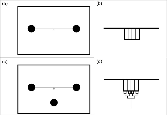
Figure 1: Example photomask designs for fabrication of microfluidic devices (black and white colors are inverted for clarity). (a) Entire field of view for a connected fracture network containing a main fracture and micro cracks. (b) Zoomed-in view of the main feature comprising a connected fracture network containing a main fracture and micro-cracks. (c) A third port is added at the bottom. (d) Zoomed-in view of the main feature comprising a connected fracture network containing a main fracture and micro-cracks along with a distribution network connecting the network to the port at the bottom of the device. Please click here to view a larger version of this figure.
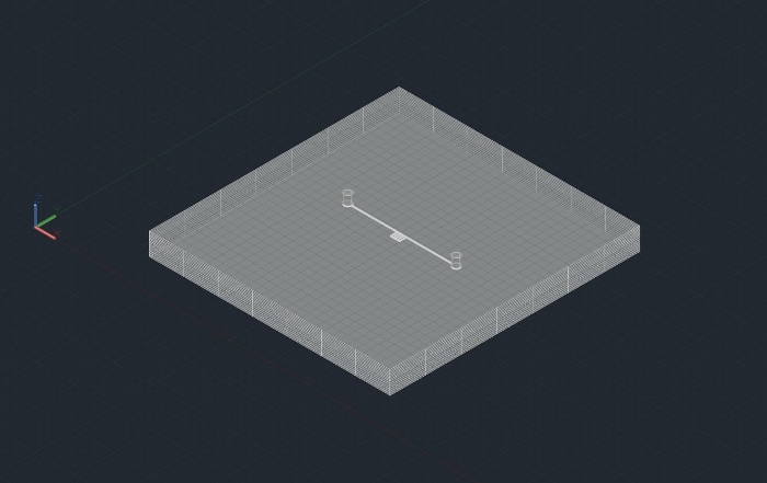
Figure 2: 3D Microfludic design used in SLE fabrication and high-pressure foam flow through microchannels. Please click here to view a larger version of this figure.
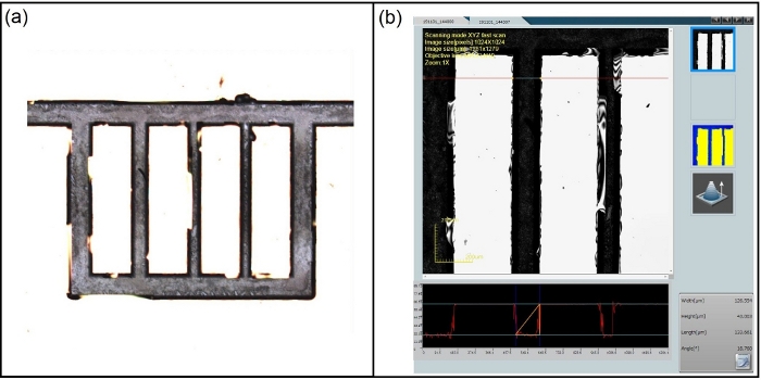
Figure 3: Examination of channel depth via confocal microscopy for substrate dipped in BD-etchant for 136 h (no sonication in this case). (a) channel overview (b) channel depth measurement (~43 μm). Please click here to view a larger version of this figure.
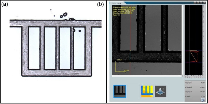
Figure 4: Examination of channel depth via confocal microscopy for a substrate with chrome layer removed after NMP rinsing. (a) Channel overview. (b) Channel depth measurement (~42.5 μm). Please click here to view a larger version of this figure.

Figure 5: Schematic of thermal bonding process. (a) Placing two glass wafers between two smooth ceramic plates. (b) Placing the ceramic plates between two metallic plates and tightening the bolts. (c) Placing the metallic and ceramic holder containing the substrates inside a programmable furnace to achieve the desired temperatures for thermal bonding. Please click here to view a larger version of this figure.
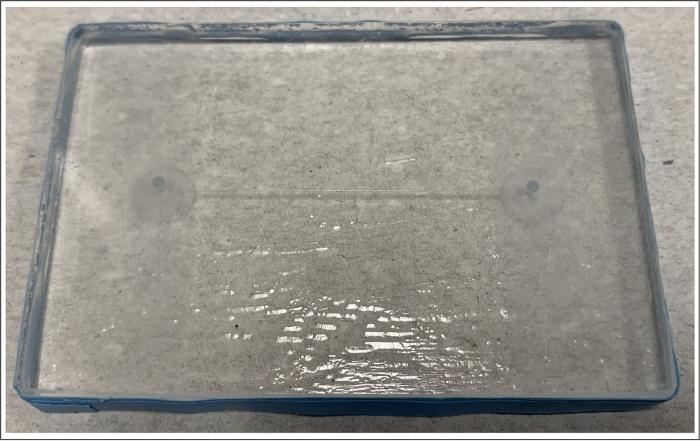
Figure 6: The completed UV-etched glass microfluidic device. Please click here to view a larger version of this figure.
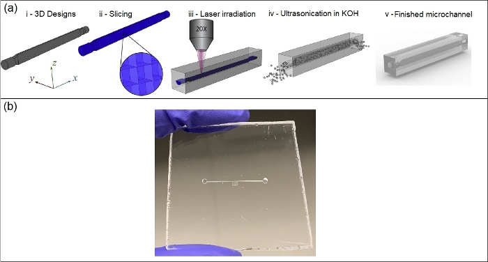
Figure 7: SLE design and fabrication process. (a) Schematic of SLE design and fabrication process (this figure has been reprinted with permission from Elsevier27), and (b) the resulting 3D printed microfluidic device. Design and fabrication steps include (a.i) designing the inner volume of channels, (a.ii) slicing the 3D model to create a z-stack of lines to define the laser path, (a.iii) laser irradiation on the polished fused silica substrate, (a.iv) preferential KOH etching of laser etched materials, and (a.v) the finished product. Please click here to view a larger version of this figure.
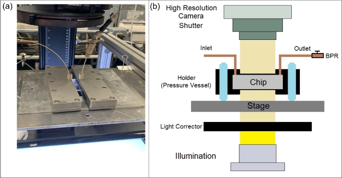
Figure 8: Microfluidic device placed inside a holder and the imaging system comprising a high-resolution camera and an illumination system. (a) A photograph of laboratory setup, and (b) schematic of a lab-on-a-chip under observation via the high-resolution camera and illumination system. Please click here to view a larger version of this figure.
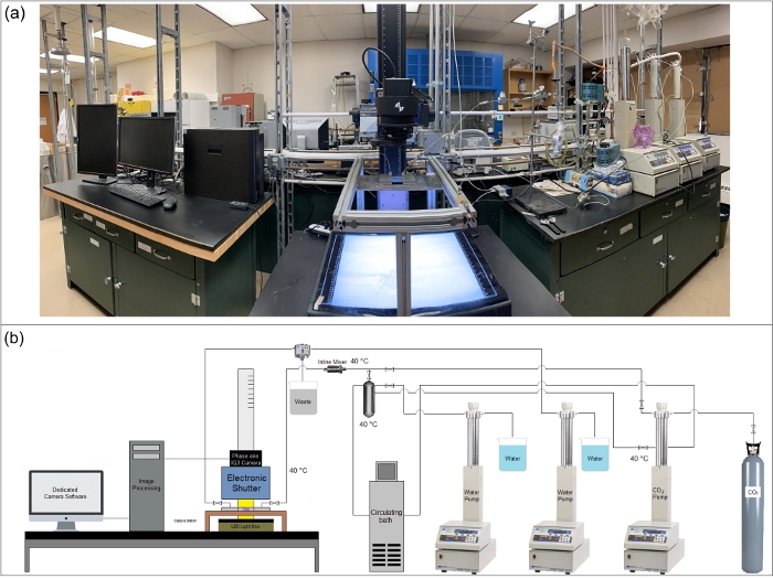
Figure 9: High-pressure scCO2 foam injection setup into a microfluidic device and a visualization system using a high-resolution camera and image processing unit. (a) photograph of laboratory setup, and (b) schematic of process flow diagram and the image processing unit. Please click here to view a larger version of this figure.
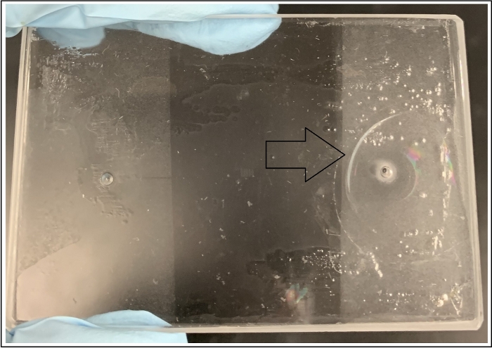
Figure 10: De-bonded device at an injection port (right entrance) as a result of mishandling the pressure profile by BPR and water pump during injection. Please click here to view a larger version of this figure.
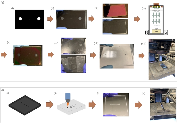
Figure 11: Comparative fabrication methods of glass microfluidic device. (a) Fabrication process for fractured media microfluidic device using photo-lithography (a.i) design for a positive photoresist, (a.ii) printed photomask on a polyester-based transparency film, (a.iii) blank and photoresist/chrome coated glass substrates, (a.iv) transferring the pattern to the substrate via UV radiation, (a.v) etched substrate, (a.vi) etched substrate after chrome layer removal and the blank substrate prepared for thermal bonding, (a.vii) thermally bonded device, and (a.viii) scCO2 injection. (b) Fabrication using the SLE technique: (b.i) design for SLE printing, (b.ii) laser irradiation on the polished fused silica substrate, (b.iii) SLE printed glass microfluidic device, and (b.iv) scCO2 injection. Please click here to view a larger version of this figure.
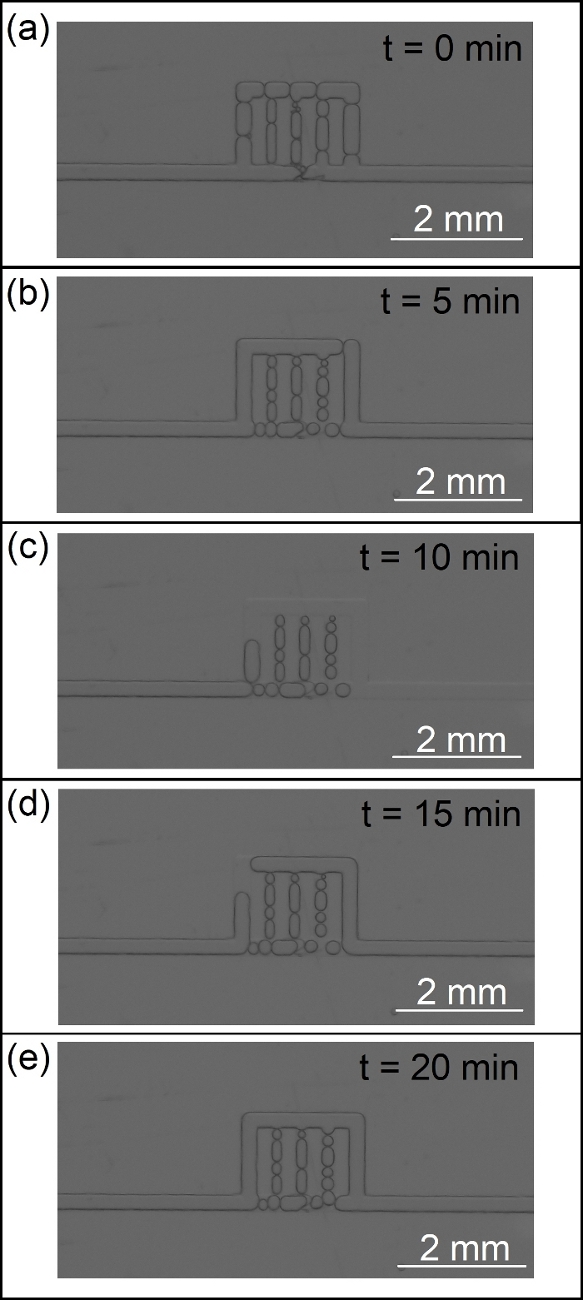
Figure 12: CO2 foam transport and stability in the UV-lithography microfluidic device (4 MPa and 40 ˚C) during the first 20 min of generation/isolation. Please click here to view a larger version of this figure.
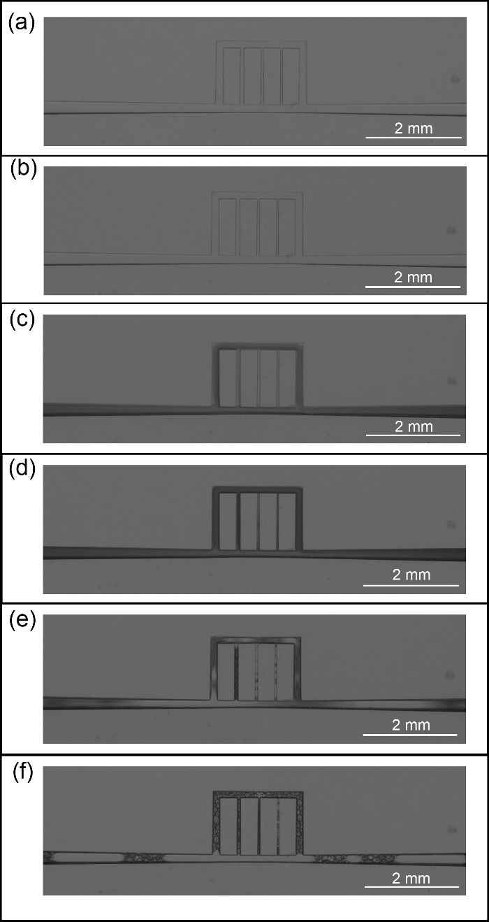
Figure 13: scCO2 foam generation in the SLE microfluidic device (7.72 MPa and 40 °C). (a) Ambient condition with no flow through the micro channels. (b) Co-injection of CO2 and aqueous phase (containing surfactant or nanoparticle) at supercritical condition. (c) Onset of scCO2 foam generation 0.5 min after start of co-injection. (d) Fully developed scCO2 foam at high flow rates (e) lowering the flow rates of co-injection to reveal the borders of multiphase. (f) Profoundly low flow rates reveal dispersed scCO2 bubbles in the aqueous phase. Please click here to view a larger version of this figure.
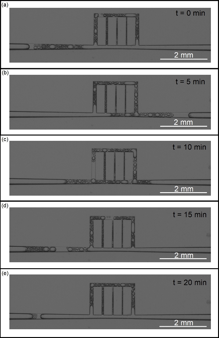
Figure 14: Visualization of foam stability under reservoir conditions (7.72 MPa and 40 ˚C) during the first 20 min of generation/isolation. Please click here to view a larger version of this figure.
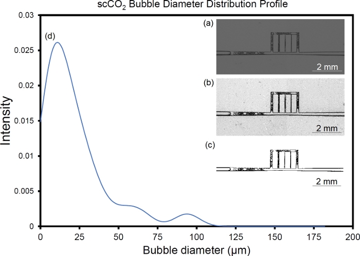
Figure 15: Analysis of foam microstructure. (a) Image of scCO2 foam flow in the fracture network, (b) post-processed image with improved brightness, contrast and sharpness, (c) binarized image using ImageJ, and (d) bubble diameter distribution profile obtained from ImageJ, particle analysis mode. Please click here to view a larger version of this figure.
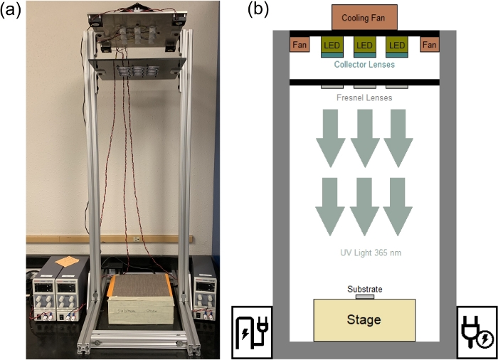
Figure 16: Illustration of in-house collimated UV light source. (a) Photograph and (b) a schematic of laboratory UV light stand containing LED light sources and a stage. Please click here to view a larger version of this figure.

Figure 17: Color-coded plot of UV intensity in a 10 x 10 cm2 area of the stage where the substrate is placed for UV exposure. UV intensity values range from 4 to 5 mW/cm2 as recorded using a UV meter. Please click here to view a larger version of this figure.
Supplementary File 1. Please click here to download this file.
Discussion
This work presents a protocol related to a fabrication platform to create robust, high-pressure glass microfluidic devices. The protocol presented in this work alleviates the need for a cleanroom by performing several of the final fabrication steps inside a glovebox. The use of a cleanroom, if available, is recommended to minimize the potential for contamination. Additionally, the choice of the etchant should be based on the desired surface roughness. The use of a mixture of HF and HCl as the etchant tends to reduce surface roughness30. This work is concerned with microfluidic platforms that enable direct, in situ visualization of transport of complex fluids in complex permeable media that faithfully represent the complex structures of subsurface media of interest. As such, this work uses a buffered etchant that enables the study of mass transfer and transport in surrogate media resembling geologic permeable media.
Design of patterns
The patterns are created using a computer aided design software (Table of Materials) and the features are intended to represent factures and microcracks to study transport and stability of foam (see Figure 1). These patterns may be printed on a high-contrast, polyester-based transparent film, or a borofloat or quartz plate (photomask). The patterns used in photolithography comprise a main channel, 127 μm in width and 2.2 cm in length, that serves as the main fracture. This channel is connected to an array of micro-fractures with various dimensions, or a permeable medium consisting of an array of circular posts, with diameters of 300 μm, that are connected to the middle of the fracture path. Additional auxiliary ports may be included in the design to help with the initial saturation of the main features, e.g., fractures.
Photoresist
This work uses a positive photoresist. As a result, the areas in the design that correspond to features that are intended to be etched on the substrate are optically transparent and the other areas obstruct the transmission of light (collimated UV light). In the case of a negative photoresists, the situation would be the opposite: the areas in the design that correspond to the features that are intended to be etched on the substrate shall be optically nontransparent.
UV light source
The patterns are transferred to the photoresist by altering its solubility as a result of its exposure to UV light. A full-spectrum, mercury-vapor lamp may serve as the UV source. The use of a collimated, narrow-band UV source, however, improves the quality and precision of the fabrication significantly. This work uses a photoresist with peak sensitivity at 365 nm, a collimated UV source consisting of an array of light emitting diodes (LED), and an exposure time of approximately 150 s. This UV source is a developed in-house and offers a low maintenance, low-divergence, collimated UV light source for lithography. The UV source consists of a square array of nine high-power LEDs with a target peak emission wavelength of 365 nm at 25 °C (3.45 mm x 3.45 mm UV LED with Ceramic substrate—see Table of Materials). A light-collecting UV lens (LED 5 W UV Lens – see Table of Materials) is used on each LED to reduce the divergence from ~70° to ~12°. The divergence is further reduced (~5°) by using a 3 x 3 array of nine converging polyvinylchloride (PVC) Fresnel lenses. The setup produces collimated and uniform UV radiation over a 3.5-inch squared area. The details of the fabrication of this low-cost light source for UV lithography is adapted from the method presented by Erickstad and co-workers25 with minor modifications15,26. Figure 16 illustrates the LED UV light source mounted on the celling of UV stand alongside the stage at the bottom for substrate UV exposure (the procedure is performed in a darkroom). The UV stage is placed 82.55 cm from the nine Fresnel lenses that are mounted on a rack 13.46 cm below the rack that houses the LEDs. As seen in Figure 16a, there are four small fans (40 mm x 40 mm x 10 mm 12 V DC Cooling Fan—see Table of Materials) on the bottom of the plate that houses the LEDs and there is a larger fan (120 mm x 38 mm 24 V DC Cooling Fan—see Table of Materials) on the top. Three variable DC power supplies (Table of Materials) are used to power the LEDs. One power supply feeds the center LED at 0.15 A, 3.3 V; one power supply feeds the four corner LEDs at 0.6 A, 14.2 V; and one power supply feeds the remaining four LEDs at 0.3 A, 13.7 V. The stage, shown schematically in Figure 16b, is divided into 1 cm2 sub-areas and the intensity of the UV light is measured in each using a UV power meter (Table of Materials) that is equipped with a 2 W 365 nm robe assembly. On average, the UV light has an average strength of 4.95 mW/cm2 with a variability characterized by a standard deviation of 0.61 mW/cm2. Figure 17 presents a color-coded plot of UV intensity map for this UV light source. The intensity over the region of 10 cm 10 cm is relatively uniform with values ranging from 4 to 5 mW/cm2 in the center of the stage where the substrate is placed and exposed to the light. For more information on the development of the in-house collimated UV-light source refer to ESI, Supplementary File 1: Figure S3, S4. The use of the UV source may be coupled with UV blocking shields/covers for its safe use. Additional safety measures may include the use of UV safety goggles (Laser Eye Protection Safety Glasses for Red and UV Lasers – (190–400 nm)), face-shields marked with the term Z87 that meets the ANSI standard (ANSI Z87.1-1989 UV certification) to provide basic UV protection (Table of Materials) lab coats and gloves to minimize the exposure.
Fabrication techniques
This work also presents a step by step roadmap for high-pressure foam injection in fabricated glass microfluidic devices using a high-resolution camera and an illumination source. Examples of CO2 and scCO2 foam microstructure and transport in microfluidic devices are also presented with relevance to fractured tight and ultra-tight formations. Direct observation of transport in these subsurface media is a challenging task. As such, the devices described in this work provide an enabling platform to study transport in permeable media under temperature and pressure conditions that are relevant to subsurface applications such as fractured media, EOR processes and aquifer remediation.
Devices used in this work are fabricated using two different techniques, namely photolithography/wet-etching/thermal-bonding and SLE. The photolithography/wet-etching/thermal-bonding technique comprises a relatively low-cost etching process using a low-maintenance, collimated UV light-source. SLE is executed using a femto-second laser source followed by removal of modified glass from the glass bulk via wet-etching. The main steps involved in the photolithography/wet-etching/thermal-bonding technique include: (i) creation of the map of the channel network, (ii) printing the design on polyester based transparency film or a glass substrate, (iii) transferring the pattern on to a chrome/photoresist coated borosilicate substrate, (iv) removal of exposed area by photo developer and chrome etchant solutions, (v) etching the patterned area of the borosilicate substrate to the desired depth, (vi) preparing a cover plate with entry holes positioned in appropriate locations, and (vii) thermal bonding of the etched substrate and the cover plate. In contrast, SLE employs a two-step process: (i) selective laser-induced printing in a transparent fused silica substrate, and (ii) selective removal of the modified materials via wet chemical etching leading to the development of three-dimensional features in the fused silica substrate. In the first step, laser radiation through the fused silica glass internally modifies the glass bulk to increase the chemical/local etch-ability. The focused laser scans inside the glass to modify a three-dimensional connected volume that is connected to one of the surfaces of the substrate.
Both techniques result in devices that are chemically and physically resistant and tolerant of high pressure and temperature conditions that correspond to subsurface systems of interest. Both techniques provide pathways to create high-precision etched micro-channels and capable lab-on-a-chip devices. The photolithography/wet-etching/thermal-bonding technique is robust in terms of the geometry of the channels and may be used to etch complex channel networks, whereas SLE is limited to relatively simple networks due to practical reasons. On the other hand, devices made with photolithography/wet-etching/thermal-bonding may be more vulnerable to breakage due to bonding imperfections, residual thermal stresses from fast heating/cooling rates during thermal bonding and structural flaws from the wet-etching process. In contrast to photolithography, SLE devices appear more resilient under high pressures (tested up to 9.65 MPa). Regardless of the fabrication technique, rapid pressure buildup rates may increase the chance of mechanical failures in microfluidic devices.
Disclosures
The authors have nothing to disclose.
Acknowledgements
The authors from the University of Wyoming gratefully acknowledge support as part of the Center for Mechanistic Control of Water-Hydrocarbon-Rock Interactions in Unconventional and Tight Oil Formations (CMC-UF), an Energy Frontier Research Center funded by the U.S. Department of Energy, Office of Science under DOE (BES) Award DE-SC0019165. The authors from the University of Kansas would like to acknowledge the National Science Foundation EPSCoR Research Infrastructure Improvement Program: Track -2 Focused EPSCoR Collaboration award (OIA- 1632892) for funding of this project. Authors also extend their appreciation to Jindi Sun from the Chemical Engineering Department, University of Wyoming for her generous help in instrument training. SAA thanks Kyle Winkelman from the University of Wyoming for his help with constructing the imaging and UV stands. Last but not the least, the authors gratefully acknowledge John Wasserbauer from microGlass, LLC for useful discussions regarding the SLE technique.
Materials
| 1/4” bolts and nuts | For fabrication of the metallic plates to sandwich the glass chip between them for thermal bonding | ||
| 3.45 x 3.45 mm UV LED | Kingbright | To emitt LED light | |
| 3D measuring Laser microscope | OLYMPUS | LEXT OLS4000 | To measure channel depths |
| 40 mm x 40 mm x 10 mm 12V DC Cooling Fan | Uxcell | To cool the UV LED lights | |
| 120 mm x 38 mm 24V DC Cooling Fan | Uxcell | To cool the UV LED lights | |
| 5 ml (6 ml) NORM-JECT Syringe | HENKE SASS WOLF | Lot #16M14CB | To rinse the chip before each experiment |
| Acetone (Certified ACS) | Fisher Chemical | Lot #177121 | For cleaning |
| Acid/ corossion resistive tweezer | TED PELLA | To handle the glass piece in corosive solutions | |
| Acid/solvent resistance tweezers | TED PELLA, INC | #53009 and #53010 | To handle the glass in corrosive solutions |
| Alloy X | AMERICAN SPECIAL METALS | Heat Number: ZZ7571XG11 | |
| Ammonium hydroxide (ACS reagent) | Sigma Aldrich | Lot #SHBG9007V | To clean the chip at the end of process |
| AutoCAD | Autodesk, San Rafael, CA | To design 2D patterns and 3D chips | |
| BD Etchant for PSG-SiO2 systems | TRANSENE | Lot #028934 | An improved buffered etch formulation for delineation of phosphosilica glass – SiO2 (PSG), and borosilica glass – SiO2 (BSG) systems |
| Blank Borofloat substrate | TELIC | CG-HF | Upper substrate for UV etching |
| Borofloat substrate with metalizations | TELIC | PG-HF-LRC-Az1500 | Lower substrate for UV etching |
| Capture One photo editing software | Phase One | To Capture/Edit/Convert the pictures taken by Phase One Camera | |
| Capture station | DT Scientific | DT Versa | To place of the chip in the field of view of the camera |
| Carbon dioxide gas (Grade E) | PRAXAIR | UN 1013, CAS Number 124-38-9 | non-aqeous portion of foam |
| Chromium etchant 1020 | TRANSENE | Lot #025433 | High-purity ceric ammonium nitrate systems for precise, clean etching of chromium and chromium oxide films. |
| Circulating baths with digital temperature controller | PolyScience | To control the brine and CO2 temperatures | |
| CO2 | Airgas | 100% pure – 001013 – CAS: 124-38-9 | For CO2/scCO2 injection |
| Computer | NVIDIA Tesla K20 Graphic Card – 706 MHz Core – 5 GB GDDR5 SDRAM – PCI Express 2.0 x16 | To process and visualize the images obtained via the Phase One camera | |
| Custom made high pressure glass chip holder | To tightly hold the chip and its connections for high pressure testing | ||
| Cutrain (Custom) | To protect against UV/IR Radiations | ||
| Deionized water (DI) | For cleaning | ||
| Digital camera with monochromatic 60 MP sensor | Phase One | IQ260 | Visualization system |
| Ethanol, Anhydrous, USP Specs | DECON LABORATORIES, INC. | Lot #A12291505J, CAS# 64-17-5 | For cleaning |
| Facepiece reusable respirator | 3M | 6502QL, Gases, Vapors, Dust, Medium | To protect against volatile solution inhalation |
| Fused Silica (UV Grade) wafer | SIEGERT WAFER | UV grade | Glass precursor for SLE printing |
| GIMP | Open-source image processing software | To characterize image texture and properties | |
| Glovebox (vinyl anaerobic chamber) | Coy | To provide a clean, dust-free environment | |
| Heated ultrasonic cleaning bath | Fisher Scientific | To accelerate the etching process | |
| Hexamethyldisilazane (HMDS) Cleanroom® MB | KMG | 62115 | Primer for photoresist coating |
| Hose (PEEK tubing) | IDEX HEALTH & SCIENCE | Natural 1/16" OD x .010" ID x 5ft, Part # 1531 | Flow connections |
| Hydrochloric acid, certified ACS plus | Fisher Chemical | Lot # 187244 | Solvent in RCA semiconductor cleaning protocol |
| Hydrogen Peroxide | Fisher Chemical | H325-500 | Solvent in RCA semiconductor cleaning protocol |
| ImageJ | NIH | To characterize image texture and properties | |
| ISCO syringe pump | TELEDYNE ISCO | D-SERIES (100DM, 500D) | To pump the fluids |
| Kaiser LED light box | Kaiser | To illuminate the chip | |
| Laser printing machine | LightFab GmbH, Germany. | FILL | Glass-SLE chip fabrication |
| Laser safety glasses | FreeMascot | B07PPZHNX4 | To protect against UV/IR Radiations |
| LED Engin 5W UV Lens | LEDiL | To emitt LED light | |
| Light Fab 3D Printer (femtosecond laser) | Light Fab | To selectively laser Etch of fused silica | |
| LightFab 3D printer | LightFab GmbH, Germany | To SLE print the fused silica chips | |
| MATLAB | MathWorks, Inc., Natick, MA | To characterize image texture and properties | |
| Metallic plates | |||
| Micro abrasive sand blasters (Problast 2) | VANIMAN | Problast 2 – 80007 | To craete holes in cover plates |
| MICROPOSIT 351 developer | Dow | 10016652 | Photoresist developer solution |
| Muffle furnace | Thermo Scientific | Thermolyne Type 1500 | Thermal bonding |
| N2 pure research grade | Airgas | Research Plus – NI RP300 | For drying the chips in each step |
| NMP semiconductor grade – 0.1μm Filtered | Ultra Pure Solutions, Inc | Lot #02191502T | Organic solvent |
| Oven | Gravity Convection Oven | 18EG | |
| Phase One IQ260 with an achromatic sensor | Phase One | IQ260 | To visulize transport in microfluidic devices using an ISO 200 setting and an aperture at f/8. |
| Photomask | Fine Line Imaging | 20,320 DPI FILM | Pattern of channels |
| Photoresist (SU-8) | MICRO CHEM | Product item: Y0201004000L1PE, Lot Number: 18110975 | Photoresist |
| Polarized light microscope | OLYMPUS | BX51 | Visual examination of micro channels |
| Ports (NanoPort Assembly) | IDEX HEALTH & SCIENCE | NanoPort Assembly Headless, 10-32 Coned, for 1/16" OD, Part # N-333 | Connections to the chip |
| Python | Python Software Foundation | To characterize image texture and properties | |
| Safety face shield | Sellstrom | S32251 | To protect against UV/IR Radiations |
| Sealing film (Parafilm) | Bemis Company, Inc | Isolation of containers | |
| Shutter Control Software | Schneider-Kreuznach | To adjust shutter settings | |
| Smooth ceramic plates | |||
| Stirring hot plate | Corning® | PC-620D | To heat the solutions |
| Sulfuric acid, ACS reagent 95.0-98.0% | Sigma Aldrich | Lot # SHBK0108 | Solvent in RCA semiconductor cleaning protocol |
| Syringe pump (Standard Infuse/Withdraw PHD ULTRA) | Harvard Apparatus | 70-3006 | To saturate the chip before each experiment |
| Torque wrench | Snap-on | TE25A-34190 | To tighten the screws |
| UV power meter | Optical Associates, Incorporated | Model 308 | To measure the intesity of UV light |
| UV power meter | Optical Associates, Incorporated | Model 308 | To quantify the strength of UV light |
| UV radiation stand (LED lights) | To transfer the pattern to glass (photoresist layer) | ||
| Vaccum pump | WELCH VACCUM TECHNOLOGY, INC | 1380 | To dry the chip |
| Variable DC power supplies | Eventek | KPS305D | To power the UV LED lights |
References
- Hyman, J. D., et al. Understanding hydraulic fracturing: a multi-scale problem. Philosophical Transactions of the Royal Society A: Mathematical, Physical and Engineering Sciences A. 13 (374), 1-15 (2016).
- Middleton, R. S., et al. Shale gas and non-aqueous fracturing fluids: Opportunities and challenges for supercritical CO2. Applied Energy. 147 (1), 500-509 (2015).
- Hosseini, H., Tsau, J., Peltier, E., Barati, R. Lowering Fresh Water Usage in Hydraulic Fracturing by Stabilizing scCO2 Foam with Polyelectrolyte Complex Nanoparticles Prepared in High Salinity Produced Water. SPE-189555-MS. , (2018).
- Gregory, K. B., Vidic, R. D., Dzombak, D. A. Water management challenges associated with the production of shale gas by hydraulic fracturing. Elements. 7, 181-186 (2017).
- Ellsworth, W. L. Injection-Induced Earthquakes. Science. 341, 1-8 (2013).
- Hosseini, H., et al. Experimental and Mechanistic Study of Stabilized Dry CO2 Foam Using Polyelectrolyte Complex Nanoparticles Compatible with Produced Water To Improve Hydraulic Fracturing Performance. Journal of Industrial and Engineering Chemistry Research. 58, 9431-9449 (2019).
- Hosseini, H., Tsau, J. S., Peltier, E., Ghahfarokhi, R. B. Highly stable scCO2-high salinity brine interface for waterless fracturing using polyelectrolyte complex nanoparticles. Abstract Paper of American Chemical Society. 256, (2018).
- Al-Muntasheri, G. A. Critical Review of Hydraulic-Fracturing Fluids for Moderate- to Ultralow- Permeability Formations Over the Last Decade. SPE Production & Operations, SPE-169552. 29 (04), 243-260 (2014).
- Tong, S., Singh, R., Mohanty, K. K. Proppant Transport in Fractures with Foam-Based Fracturing Fluids. SPE-187376-MS. , (2017).
- Fernø, M. A., Eide, &. #. 2. 1. 6. ;., Steinsbø, M., Langlo, S. A. W., Christophersen, A., Skibenes, A., et al. Mobility control during CO2 EOR in fractured carbonates using foam: Laboratory evaluation and numerical simulations. Journal of Petroleum Science and Engineering. 135, 442-451 (2015).
- Middleton, R., Viswanathan, H., Currier, R., Gupta, R. CO2 as a fracturing fluid: Potential for commercial-scale shale gas production and CO2 sequestration. Energy Procedia. 63, 7780-7784 (2014).
- Guo, F., Aryana, S. A. Improved sweep efficiency due to foam flooding in a heterogeneous microfluidic device. Journal of Petroleum Science and Engineering. 164, 155-163 (2018).
- Nazari, N., Hosseini, H., Jyun-Syung, T., Shafer-Peltier, K., Marshall, C., Ye, Q., Ghahfarokhi, R. B. Development of Highly Stable Lamella Using Polyelectrolyte Complex Nanoparticles: An Environmentally Friendly scCO2 Foam Injection Method for CO2 Utilization Using EOR. Fuel. 261, 11636 (2020).
- Nguyen, V. H., Kang, C., Roh, C., Shim, J. J. Supercritical CO2 -Mediated Synthesis of CNT@Co3O4 Nanocomposite and Its Application for Energy Storage. Industrial and Engineering Chemistry Research. 55, 7338-7343 (2016).
- Guo, F., Aryana, S. A., Wang, Y., Mclaughlin, J. F., Coddington, K. Enhancement of storage capacity of CO2 in megaporous saline aquifers using nanoparticle-stabilized CO2 foam. International Journal of Greenhouse Gas Control. 87, 134-141 (2019).
- Guo, F., Aryana, S. An experimental investigation of nanoparticle-stabilized CO2 foam used in enhanced oil recovery. Fuel. 186, 430-442 (2016).
- Guo, F., He, J., Johnson, A., Aryana, S. A. Stabilization of CO2 foam using by-product fly ash and recyclable iron oxide nanoparticles to improve carbon utilization in EOR processes. Sustainable Energy and Fuels. 1, 814-822 (2017).
- Wang, Y., Shahvali, M. Discrete fracture modeling using Centroidal Voronoi grid for simulation of shale gas plays with coupled nonlinear physics. Fuel. 163, 65-73 (2016).
- Tiggelaar, R. M., Benito-Lopez, F., Hermes, D. C., Rathgen, H., Egberink, R. J. M., Mugele, F. G., Reinhoudt, N. D., van den Berg, A., Verboom, W., Gardeniers, H. J. G. E. Fabrication, mechanical testing and application of high-pressure glass microreactor chips. Chemical Engineering Journal. 131, 163-170 (2007).
- Marre, S., Adamo, A., Basak, S., Aymonier, C., Jensen, K. F. Design and Packaging of Microreactors for High Pressure and High Temperature Applications. Industrial and Engineering Chemistry Research. 49, 11310-11320 (2010).
- Paydar, O. H., Paredes, C. N., Hwang, Y., Paz, J., Shah, N. B., Candler, R. N. Characterization of 3D-printed microfluidic chip interconnects with integrated O-rings. Sensors Actuators A: Physical. 205, 199-203 (2014).
- Jiménez-Martínez, J., et al. Pore-scale mechanisms for the enhancement of mixing in unsaturated porous media and implications for chemical reactions. Geophysical Research Letters. 42, 5316-5324 (2015).
- Jiménez-martínez, J., Porter, M. L., Hyman, J. D., Carey, J. W., Viswanathan, H. S. Mixing in a three-phase system: Enhanced production of oil-wet reservoirs by CO2 injection. Geophysical Research Letters. 43, 196-205 (2016).
- Rognmo, A. U., Fredriksen, S. B., Alcorn, Z. P. Pore-to-Core EOR Upscaling for CO2 Foam for CCUS. SPE Journal. 24, 1-11 (2019).
- Erickstad, M., Gutierrez, E., Groisman, A. A low-cost low-maintenance ultraviolet lithography light source based on light-emitting diodes. Lab on a Chip. 15, 57-61 (2015).
- Guo, F., Aryana, S. A. An Experimental Investigation of Flow Regimes in Imbibition and Drainage Using a Microfluidic Platform. Energies. 12 (7), 1-13 (2019).
- Burshtein, N., Chan, S. T., Toda-peters, K., Shen, A. Q., Haward, S. J. 3D-printed glass microfluidics for fluid dynamics and rheology. Current Opinion in Colloid & Interface Science. 43, 1-14 (2019).
- Wang, Y., Aryana, S. A., Banerjee, S., Barati, R., Patil, S. Creation of Saturation Maps from Two-Phase Flow Experiments in Microfluidic Devices. Advances in Petroleum Engineering and Petroleum Geochemistry. Advances in Science, Technology & Innovation. , 77-80 (2019).
- Hermans, M., Gottmann, J., Riedel, F. Selective, Laser-Induced Etching of Fused Silica at High Scan-Speeds Using KOH. Journal of Laser Micro/Nanoengineering. 9, 126-131 (2014).
- Iliescu, C., Jing, J., Tay, F. E. H., Miao, J., Sun, T. Characterization of masking layers for deep wet etching of glass in an improved HF/HCl solution. Surface & Coatings Technology. 198, 314-318 (2005).

