Focused Ion Beam Fabrication of LiPON-based Solid-state Lithium-ion Nanobatteries for In Situ Testing
Summary
A protocol for the fabrication of electrochemically active LiPON-based solid-state lithium-ion nanobatteries using a focused ion beam is presented.
Abstract
Solid-state electrolytes are a promising replacement for current organic liquid electrolytes, enabling higher energy densities and improved safety of lithium-ion (Li-ion) batteries. However, a number of setbacks prevent their integration into commercial devices. The main limiting factor is due to nanoscale phenomena occurring at the electrode/electrolyte interfaces, ultimately leading to degradation of battery operation. These key problems are highly challenging to observe and characterize as these batteries contain multiple buried interfaces. One approach for direct observation of interfacial phenomena in thin film batteries is through the fabrication of electrochemically active nanobatteries by a focused ion beam (FIB). As such, a reliable technique to fabricate nanobatteries was developed and demonstrated in recent work. Herein, a detailed protocol with a step-by-step process is presented to enable the reproduction of this nanobattery fabrication process. In particular, this technique was applied to a thin film battery consisting of LiCoO2/LiPON/a-Si, and has further been previously demonstrated by in situ cycling within a transmission electron microscope.
Introduction
Focused ion beams (FIB) have been used chiefly for transmission electron microscopy (TEM) specimen preparation and circuit editing1,2. Nanofabrication using FIB has progressed significantly during the last two decades with much focus on semiconductor materials3. Despite its importance to scientific advances, major concerns with FIB techniques remain, including surface damage, re-deposition, and preferential sputtering due to high current density4,5. There have been several articles on FIB damaging bulk materials during the preparation of TEM specimens and several methods to reduce this damage have been proposed6,7,8,9. However, FIB fabrication of active devices that consist of multiple layers with different functionality is still limited.
For solid-state devices, especially in the field of energy storage, interfaces play a crucial role, and the solid-solid interface is most often seen as a dominant source of impedance10. These interfaces are particularly difficult to characterize, due to a combination of their buried nature and data convolution in the presence of multiple interfaces in a single device. The fabrication of fully solid-state nanobatteries is critical to probe and understand the dynamic nature of these interfaces, which ultimately impact the electrochemical processes in batteries. Thin film batteries based on lithium phosphorous oxynitride (LiPON) were demonstrated more than two decades ago and are currently commercialized11. Although FIB fabrication of electrochemically active nanobatteries from a thin film battery is critical for enabling in situ evaluation of interfaces, most attempts to fabricate nanobatteries using FIB fail to retain electrochemical activity due to short-circuiting12. Initial attempts at in situ cycling thinned only a small portion of the nanobattery, to observe the lithium distribution by electron holography13.
More recent work has demonstrated the successful FIB fabrication of electrochemically active nanobatteries, which enabled both ex situ and in situ scanning transmission electron microscopy (STEM) and electron energy loss spectroscopy (EELS) characterization of interfacial phenomenon14,15. Important FIB fabrication parameters that help to retain electrochemical activity have been indicated by Santhanagopalan et al.14, and a detailed protocol is presented in this manuscript. This procedure is based on a model LiCoO2/LiPON/a-Si battery, but will ultimately enable the exploration of further thin film battery chemistries.
Protocol
1. Preparation of Sample and System
- Attain a complete thin film battery consisting of an Al2O3 substrate (500 µm thick), a gold cathode current collector (100 – 150 nm thick, DC sputtered), a LiCoO2 cathode (2 µm thick, RF sputtered), a LiPON electrolyte (1 µm thick, RF sputtered), an amorphous silicon anode (80 nm thick, RF sputtered), and a Cu anode current collector (100 nm, DC sputtered)16,17.
- Mount a complete thin film battery on a 25-mm diameter aluminum SEM stub, and use a copper tape to electrically connect the cathode current collector to the SEM stub to minimize charging effects.
- Prior to pumping down the chamber, confirm a low-noise electrical pathway exists to the copper grid, which the nanobattery will be mounted on and will serve as the conductive pathway to the cathode (Figure 1).
- Connect the cathode lead to the stage through a shielded electrical feedthrough, as is present in systems equipped for electron beam induced current (EBIC) measurements with the appropriate connection type. Internally, connect the feedthrough to the stage with a shielded wire with an exposed tip; the method of securing the exposed wire tip will depend on the sample stage type, and, here, it is held in place by an unused stage set screw.
- Alternatively, and depending on the configuration of the grounding circuit of the instrument's stage, connect the cathode lead of the potentiostat to the stage ground using a BNC cable as shown in Figure 1.
- Perform the low-current noise test using the potentiostat in constant current mode. Apply the current with which in situ cycling is to be performed, and observe the accuracy and precision of the measured current.
NOTE: Using the configuration described in 1.3.1, a measured current of 1 pA ± 0.1 pA was achieved.
- Similarly, create a conductive pathway from the micromanipulator tip to the outside of the probe by connecting the anode lead of the potentiostat to the micromanipulator ground using a BNC cable or an alligator clip as shown in Figure 1.
- As in step 1.3.3, perform the low-current noise test using the potentiostat in constant current mode.
NOTE: Using the connections described in step 1.4, the minimum stable current achieved was 10 pA ± 1 pA, due to unshielded grounds connected to the micromanipulator.
- As in step 1.3.3, perform the low-current noise test using the potentiostat in constant current mode.
2. Lift-out of the Nanobattery
- Load the sample into the SEM/FIB chamber and pump down to system specified high vacuum (≤10-5 mbar) before turning on the electron beam and ion beam imaging.
- Focus the electron beam on the thin film battery surface and determine the eucentric height using standard SEM/FIB procedures1.
- Tilt the sample such that the ion beam is normal to the battery surface (here 52° sample tilt), and deposit a 1.5 to 2 µm thick layer of FIB-deposited organometallic platinum on the top current collector of the thin-film battery using an ion beam current of around 0.3 nA and dwell time of 200 ns over an area of 25 x 2 µm (Figure 2).
- Set ion beam voltage to 30 kV and ion beam dwell time to 100 ns for the remainder of the experimental protocol.
- Use a step-pattern cross-sectional FIB milling option, as provided in the FIB software, to expose the nanobattery stack around the Pt-deposit, as in TEM lamella preparation1. Select a milling current ≤2.8 nA. Input a mill depth extending at least 1 µm beneath the active thin film battery (Z = 5 µm in this case), a cross-sectional width (X) of 25 µm and a cross sectional height (Y) of 1.5 x Z (here, Y = 7.5 µm). Afterwards, the battery cross-section is exposed, to be viewed in SEM (here, the electron beam is 52° from surface normal) as in Figure 3.
NOTE: The actual milled depth is thin film battery dependent. - Use a cross-section cleaning procedure, provided in the FIB software, where the ion beam incrementally rasters closer to the surface being cleaned, with an ion beam current ≤0.3 nA to clean off re-deposited material and clearly expose the layered structure (Figure 3).
- Perform a series of rectangle under-cuts (also called J-cuts or U-cuts) at a stage tilt of 0° and beam current ≤2.8 nA to isolate the majority of the nanobattery2. Make under-cuts consisting of i) a lower rectangle 0.5 x 25 µm below the Au current collector onto the Al2O3 substrate, ii) a vertical rectangle 0.5 µm wide (X) and through the entirety of the nanobattery thickness (Y), and iii) a vertical rectangle 0.5 µm wide (X) and with a height less than the nanobattery thickness (Y – 2.5 µm) around the Pt-coated nanobattery as in Figure 4a. These three under-cuts should be performed in parallel mode (simultaneously milled), to prevent re-deposition of material within the under-cut regions.
- Rotate the sample 180° and perform the same horizontal undercut as in step 2.5. This isolates the bottom and sides of the nanobattery except for the remaining connected region.
- Rotate the sample 180°. Insert the micromanipulator to the park position specified in the control software, then slowly bring it in contact with the nanobattery using the x-y-z movement of the software.
- Fix the micromanipulator to the Pt region on top of the nanobattery by ion-beam depositing 0.5 µm thick Pt using a 30 keV ion beam with a current of 10 pA over an area of 2 x 1 µm.
- Ion mill the remaining connected portion of the nanobattery with a beam current around 1 nA, and raise the nanobattery vertically with the micromanipulator (Figure 4b).
- Mount the nanobattery on a Cu FIB lift-out grid with 2 µm thick ion-beam deposited Pt using a 30 keV ion beam with a current of 0.28 nA over an area of 10 x 5 µm.
- Ion mill away the connection between the micromanipulator and nanobattery using a 30 keV ion beam with a current of 0.28 nA over an area of 1 x 1 µm to a depth of 2 µm, leaving a freestanding section attached to the Cu grid (Figure 5)1.
NOTE: The Cu lift-out grid provides a flat base for mounting the nanobattery as well as serving as a conductive pathway between the stage and the nanobattery.
3. Cleaning and Cycling the Nanobattery
- Tilt the sample such that the ion beam is normal to the battery surface and use a cross-sectional cleaning procedure (see step 2.4) to remove re-deposited material over a 5 µm wide section of the nanobattery near the Cu grid, leading to a clear view of individual layers of the nanobattery (Figure 6a).
NOTE: Re-deposited material from previous milling steps must be removed from the grid-mounted nanobattery to expose the electrochemically active core of the nanobattery and prevent shorting. - Deposit 500 nm thick FIB-Pt using a 30 keV beam with a current of 0.1 nA over an area of 1 x 2 µm to create an electrical contact between the cathode current collector and the metallic grid, which is electrically connected to the stage (Figure 6b).
- Tilt the sample to 0° and, using an ion beam current of 1 nA, make a rectangular cut 3 µm wide and deep enough (Z ~ 2 µm) to completely remove the anode current collector and electrolyte, isolating the anode from the Cu grid (Figure 6c).
- Use the cross-section cleaning procedure (see step 2.4) with an ion beam current around 0.1 nA to remove the re-deposited material around all sides of the nanobattery cross-section until all the individual layers are distinctly visible as shown in Figure 6d.
- Insert the micromanipulator to the park position and, using the control software, bring the micromanipulator in contact with the Pt above the anode current collector. Ion beam deposit 0.2 µm thick Pt using a 30 keV ion beam with a current of 10 pA over an area of 2 x 1 µm to "weld" connect the micromanipulator and current collector ( Figure 6d)1.
- Run the potentiostat in galvanostatic cycling mode. Current parameters used depend on the ultimate cross-sectional area of the fabricated nanobattery and desired C-rate, but will generally be on the order of a few nA. We select charge and discharge currents such that the current density is on the order of tens of µA/cm2. For LiCoO2-based thin film batteries, the voltage range is 2.0 and 4.2 V.
Representative Results
A representative solid-state Li-ion nanobattery fabrication process is shown step-by-step in the protocol referencing Figures 1-7.
Figure 8 shows in situ testing of the electrochemical charging profiles of two cells that were fabricated. Both profiles clearly show a 3.6 V plateau corresponding to LiCoO2-Si full cell chemistry and oxidation of Co3+ → Co4+. Cell-1 (Figure 8a) was tested at a lower current density (50 µA/cm2) limiting the charge capacity to 12.5 µAh/cm2. Cell-2 (Figure 8b) presents a charging profile at a higher current density, 1.25 mA/cm2, that was limited by the upper cut-off voltage of 4.2 V. The capacity recorded was about 105 µAh/cm2, close to the theoretical capacity of Cell-2 (110 – 120 µAh/cm2). The first discharge capacity of the nanobatteries has been poor while the subsequent cycle capacities (both charge and discharge) were limited due to the first cycle irreversibility. The discharge process of nanobatteries is still not optimized, however, a representative charge-discharge profile at a current density of 60 µA/cm2 is presented in Figure 9. The charge capacity was limited to 30 min and the discharge was limited to 2 V, and it is evident that the reversibility is about 35%. Though the reversibility is a lot better than what is reported in the literature14, further optimization is necessary.
If the voltage profile is not consistent with the thin film battery chemistry, this is likely due to either beam damage or shorting from re-deposited material. Figure 10 shows a voltage profile consistent with shorting where the voltage is constant and proportional to the applied current. The ion-beam image confirms that there is re-deposited material along the edge. The micromanipulator must be removed and further cross-sectional cleaning steps are needed to remove this material. This cleaning procedure decreases the nanobattery cross-section, so the current density should be corrected accordingly.
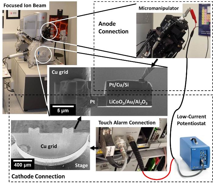
Figure 1: Electrical connection schematic. A potentiostat is connected to the FIB nanobattery via external connections: 1) the negative terminal of the potentiostat to the disconnected ground of the micromanipulator needle; 2) the cathode side to either an electrically shielded vacuum feedthrough or a direct connection to the stage ground such as a touch alarm circuit (shown). Internal connections are made between the tip of the micromanipulator and the anode, and between the cathode and stage through a copper TEM lift-out grid. Please click here to view a larger version of this figure.
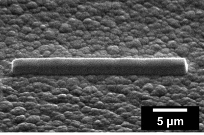
Figure 2: Pt deposition. SEM image of the Pt protective cap deposited on the thin film battery surface to avoid damage and making contact. Please click here to view a larger version of this figure.
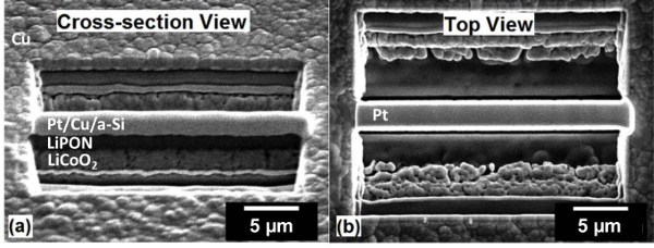
Figure 3: Nanobattery cross-section. SEM images of the nanobattery lamella after cross-sectional cutting at (a) 52° cross-section view and (b) and 0° top view. Please click here to view a larger version of this figure.
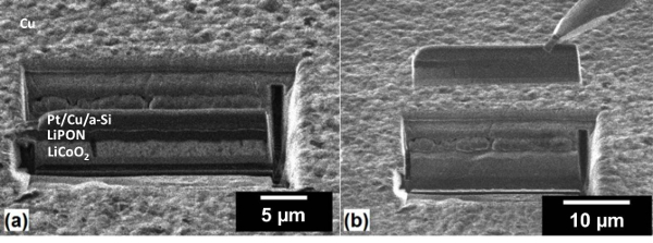
Figure 4: Nanobattery liftout. Ion-beam images of (a) the lamella with under-cut and (b) lift-out of the isolated nanobattery by the micromanipulator. Please click here to view a larger version of this figure.
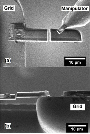
Figure 5: Nanobattery mounting. (a) Ion-beam and (b) SEM image of welding the lifted nanobattery to the copper TEM grid. Please click here to view a larger version of this figure.
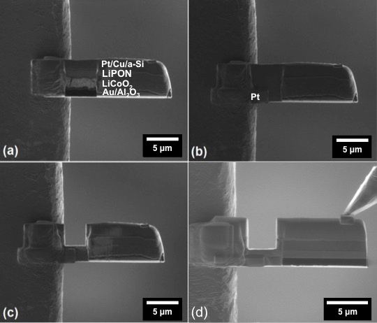
Figure 6: Nanobattery cleaning. Ion-beam images of (a) cleaning one of the nanobattery cross-sections, (b) electrically connecting the grid and cathode current collector by Pt deposition, (c) cut to isolate anode from the TEM grid, and (d) cleaning the cross-section of the front, back, and sides to remove all re-deposited material. Final contact is made to the anode using the micromanipulator for biasing. Please click here to view a larger version of this figure.
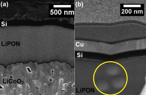
Figure 7: Nanobattery damage. SEM images of a nanobattery cross-section with (a) undamaged LiPON layer and (b) imaging at higher magnification induced damage in the LiPON layer indicated by the circle. High dwell time electron beam imaging produces visible changes in the LiPON electrolyte. Please click here to view a larger version of this figure.
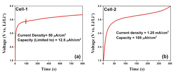
Figure 8: Nanobattery charging data. FIB fabricated nanobattery electrochemical charging profile at different current densities with (a) the capacity limited to 12.5 µAh/cm2 and (b) the voltage limited to a 4.2 V cut-off. Please click here to view a larger version of this figure.
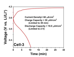
Figure 9: Nanobattery cycling profile. FIB fabricated nanobattery electrochemical charging and discharging profiles at a current density of 60 µA/cm2. Please click here to view a larger version of this figure.
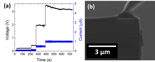
Figure 10: Shorted nanobattery. (a) Voltage profile of a nanobattery that had not been cleaned properly resulting in shorting from re-deposited material and (b) the cross sectional ion-beam image. Please click here to view a larger version of this figure.
Discussion
As demonstrated by our results, the technique described produces electrochemically active nanobatteries lifted out from a larger thin-film battery. Such techniques have enabled both ex situ and in situ STEM/EELS characterization of the buried interfaces by galvanostatically biasing the nanobattery. This allows unprecedented high-resolution characterization of quantitative chemical phenomena linked to the electrochemical state of charge. However, to achieve these results, a number of specific obstacles must be overcome.
Before beginning FIB processing, constant current testing should be conducted to ensure that there is a low-noise electrical pathway to the cathode and anode of the nanobattery. Cathode-side testing may be performed with the FIB chamber vented. Before pumping down the chamber for nanobattery fabrication, the positive terminal should be connected as if performing the experiment (either through a vacuum feedthrough or stage ground), and the negative terminal connected directly to the stage. Note that if using the touch alarm as a stage connection, the touch alarm capability of the instrument may be disabled, and the connection should only be made when no further tilting of the stage is necessary. However, here the test will require the system to be under vacuum, and the current will pass through both the micromanipulator and the stage circuit. The micromanipulator can be electrically adhered with Pt to the copper grid for constant current noise tests. If current resolution issues persist, contact your vendor for information on how to decouple the stage from the system ground.
For this technique to work, it is critical to use the provided ion beam specifications to minimize damage to the solid-electrolyte LiPON. LiPON is highly sensitive to prolonged exposure to (i) humid atmospheric conditions, (ii) electron beam, and (iii) ion beams. Hence the solid-state nanobattery fabrication process requires minimization of exposure to all three of these conditions. Pre- and post-fabrication exposure to atmospheric conditions should be absolutely minimized. The in situ FIB cycling process described was developed as a solution to minimize this exposure. During and after fabrication, electron beam imaging should be limited, as it damages the solid-electrolyte. Similarly, ion beam imaging should also be limited to avoid degradation of the electrolyte and other active components as well. The specific milling files and times are based on the equipment outlined in the table of materials/equipment for specific reagents, equipment, and manufacturers; this may vary between FIB instruments, and modifications may be required when using another instrument.
Of all parameters in the FIB fabrication of a nanobattery, the most critical considerations are the use of low beam current and dwell time to minimize damage14. Whenever required, imaging is performed with electrons at low pixel dwell times and with the ion beams at lower beam current (usually in pA) and low dwell time (100 ns). Most of the time, high dwell time electron beam imaging produces visible changes on the LiPON electrolyte. Figure 7a shows an undamaged LiPON and further imaging with an electron beam induces damage to the LiPON layer as shown in Figure 7b. This damage is irreversible resulting in a contrast change and will render the nanobattery electrochemically inactive.
Further, for electrochemical cycling, proper care must be taken to make electrical contact between the cathode current collector and the grid properly (Figure 6b). It is similarly important to maintain the micromanipulator contact to the anode (Figure 6); as seen in Figure 8a, at around 150 s, a spike in the electrochemical data corresponds to a vibration induced contact issue with the anode. Given the potential for instability of the micromanipulator-anode contact, the in situ testing time is minimized by limiting the nanobattery capacity, in turn reducing the charging time.
If the voltage profile is not consistent with the thin film battery, the cleaning procedure is repeated as there is likely some re-deposition causing shorting issues (Figure 10). The anode isolation step in particular is a large source of re-deposited material. This cleaning procedure decreases the nanobattery cross-section, so the current density should be corrected accordingly. It is noted that ion beam damage cannot be completely avoided and it is limited to between a few nm to a maximum of 25 nm into the surface, as calculated from ion scattering simulations SRIM program for 30 keV Ga+ into the electrode materials18. Low energy processing can reduce the damage to a large extent19. The FIB process demonstrated here is unique, and fabrication, manipulation, and in situ testing of nanodevices is enabled by FIB-SEM dual beam systems. It is possible to extend the process to any other battery chemistries and other nanoscale devices.
It is important to note that the specific parameters provided in this protocol may not directly transfer well to alternate electrochemical systems. LiPON was determined to be sensitive to thermal effects from the ion beam under high scanning rates. However, other electrolytes may suffer from other sensitivities. Similarly, although the material system tested in this protocol showed good electrochemistry after Ga+ ion milling, other materials systems may be more susceptible to ion straggle and implantation. As such, more exploration of the parameter space may be required for alternate material systems. More sensitive materials such as sulfides may perform poorly after ion milling, though this area of research is largely unexplored with advanced characterization techniques. Realistically, these parameters will translate to most material systems of interest, as modern solid electrolytes are generally crystalline and more robust than LiPON. Despite these potential limitations, the technique will be applied to new material systems, offering the potential to discover alternate interfacial phenomena, ultimately uncovering impedance mechanisms. A natural follow-up to this technique is the observation of electrochemical cycling in the TEM. This has been performed on the system described in this protocol, and uncovered previously unseen behavior at these interfaces. This technique will enable the observation of alternate forms of impedance.
Disclosures
The authors have nothing to disclose.
Acknowledgements
The authors acknowledge funding support for the development of all-solid-state batteries and in situ FIB and TEM holder development by U.S. Department of Energy, Office of Basic Energy Sciences, under award number DE-SC0002357. The collaboration with national laboratories is made possible with partial support of the Northeastern Centre for Chemical Energy Storage, an Energy Frontier Research Centre funded by the U.S. Department of Energy, Office of Basic Energy Sciences under the award number DE-SC0001294. This research used resources of the Center for Functional Nanomaterials, which is a U.S. DOE Office of Science Facility, at Brookhaven National Laboratory under Contract No. DE-SC0012704. This work was performed in part at the San Diego Nanotechnology Infrastructure (SDNI), a member of the National Nanotechnology Coordinated Infrastructure, which is supported by the National Science Foundation (Grant ECCS-1542148). FIB work was performed in part at the UC Irvine Materials Research Institute (IMRI), using instrumentation funded in part by the National Science Foundation Center for Chemistry at the Space-Time Limit (CHE-082913). We thank Nancy Dudney, Oak Ridge National Laboratory for providing us the thin-film batteries. J.L. acknowledges support from the Eugene Cota-Robles Fellowship Program and D.S is thankful to SERB, India for Ramanujan Fellowship (SB/S2/RJN-100/2014).
Materials
| Biologic SP-200 Potentiostat | Biologic Science Instruments | SP-200 | Ultra Low Current Option needed for pA current resolution |
| FEI Scios DualBeam FIB/SEM | FEI | Current noise improves with a shielded stage feedthrough | |
| SEM Stub: Large Ø25.4mm x 9.5mm pin height | Ted Pella | 16144 | Or equivalent |
| PELCO Colloidal Silver Paste, Conductive | Ted Pella, Inc. | 16032 | Or equivalent |
| PELCO® FIB Lift-Out TEM Grids | Ted Pella | 10GC04 | Or equivalent |
References
- Giannuzi, L. A., Stevie, F. A. . Introduction to focused ion beams: Instrumentation, theory, techniques and practice. , (2005).
- Mayer, J., Giannuzi, L. A., Kamino, T., Michael, J. TEM sample preparation and FIB-induced damage. MRS Bulletin. 32 (5), 400-407 (2007).
- Pellerin, J. G., Griffis, D. P., Russeli, P. E. Focused ion beam machining of Si, GaAs and InP. J. Vac. Sci. Technol. B. 8, 1945-1950 (1990).
- Rubanov, S., Munroe, P. R. Investigation of the structure of damage layers in TEM samples prepared using a focused ion beam. J. Mater. Sci. Lett. 20 (13), 1181-1183 (2001).
- Lugstein, A., Basnar, B., Bertagnolli, E. Study of focused ion beam response of GaAs in the nanoscale regime. J. Vac. Sci. Technol. B. 20, 2238-2242 (2002).
- Kato, N. I. Reducing focused ion beam damage to transmission electron microscopy samples. J. Elect. Micro. 53 (5), 451-458 (2004).
- Bals, S., Tirry, W., Geurts, R., Yang, Z., Schryvers, D. High quality sample preparation by low kV FIB thinning for analytical TEM measurements. Microsc. Microanal. 13 (2), 80-86 (2007).
- Miyajima, N., et al. Combining FIB milling and conventional argon ion milling techniques to prepare high-quality site-specific TEM samples for quantitative EELS analysis of oxygen in molten iron. J. Elect. Microsc. 238 (3), 200-209 (2010).
- Scahaffer, M., Schaffer, B., Ramasse, Q. Sample preparation for atomic-resolution STEM at low voltages by FIB. Ultramicroscopy. 114, 62-71 (2012).
- Wang, Z., et al. Effects of cathode electrolyte interfacial (CEI) layer on long term cycling of all-solid-state thin-film batteries. J. Power Sources. 324, 349-357 (2016).
- Bates, J. B., Dudney, N. J., Gruzalski, G. R., Zuhr, R. A., Choudhury, A., Luck, C. F., Robertson, J. D. Fabrication and characterization of amorphous lithium electrolyte thin films and rechargeable thin-film batteries. J. Power Sources. 43, 103-110 (1993).
- Brazier, A., Dupont, L., Dantras-Laffont, L., Kuwata, N., Kawamua, J., Tarascon, J. M. First cross-section observation of an all-solid-state lithium ion “nanobattery” by transmission electron microscopy. Chem. Mater. 20 (6), 2352-2359 (2008).
- Yamamoto, A., et al. Dynamic visualization of the electric potential in an all-solid-state rechargeable lithium battery. Angew. Chem. Int. Ed. 49 (26), 4414-4417 (2010).
- Santhanagopalan, D., et al. Interface limited lithium transport in solid-state batteries. J. Phys. Chem. Lett. 5 (2), 298-303 (2014).
- Wang, Z., et al. In situ STEM-EELS observation of nanoscale interfacial phenomena in all-solid-state batteries. Nano Lett. 16 (6), 3760-3767 (2016).
- Jang, Y. -. I., Dudney, N., Blom, D. A., Allard, L. F. High-voltage cycling behavior of thin-film LiCoO2 cathodes. J. Electrochem. Soc. 149 (11), 1442-1447 (2002).
- Neudecker, B. J., Zuhr, R. A., Bates, J. B. Lithium silicon tin oxynitride (LiySiTON): high-performance anode in thin-film lithium ion batteries for microelectronics. J. Power Source. 81, 27-32 (1999).
- Ziegler, J. F. SRIM-2003. Nucl. Instrum. Methods Phys. Res. B. 219, 1027-1036 (2004).
- Bals, S., Tirry, W., Geurts, R., Yang, Z., Schryvers, D. High quality sample preparation by low kV FIB thinning for analytical TEM measurements. Microsc. Microanal. 13 (2), 80-86 (2007).

