Iron Nanowire Fabrication by Nano-Porous Anodized Aluminum and its Characterization
Summary
In this work, we describe a protocol to fabricate iron nanowires, including the formation of the porous alumina membrane that is used as the template, electrodeposition into templates using electrolyte solution, and the release of the nanowires into the solution.
Abstract
Magnetic nanowires possess unique properties that have attracted the interest of different fields of research, including basic physics, biomedicine, and data storage. We demonstrate a fabrication method for iron (Fe) nanowires via electrochemical deposition into anodic alumina oxide (AAO) templates. The templates are fabricated by anodization of aluminum (Al) discs, and the pore length and diameter are controlled by changing the anodizing conditions. Pores with an average diameter of around 120 nm are created using oxalic acid as the electrolyte. Using this method, cylindrical nanowires are synthesized, which are released by dissolving the alumina using a selective chemical etchant.
Introduction
Cylindrical magnetic nanowires have attracted an enormous amount of interest in the last decade for a variety of promising applications. Nanowires are novel materials that possess unique properties, mainly due to a high aspect ratio and shape anisotropy1. Because of these properties, nanowires are considered unique systems and excellent model objects for a number of practical applications: flow sensors2, magnetic separation3, bio-inspired tactile sensors4, energy harvesting5, cancer treatments2,6, drug delivery7,8, and MRI contrast agents3,9. Nanowires are also considered ideal for other applications: magnetic force microscopy10, giant magnetoresistance11, spin transfer torque12,13, and data storage devices14,15.
In order to exploit these nanowires to their full advantage, a reproducible fabrication method that yields nanowires of high quality and specific properties is required. The anodization of aluminum produces self-organized, highly ordered cylindrical pores with controllable pore diameters. Because of this, AAO templates are preferred in nanotechnology applications over expensive lithographic techniques. Using these membranes as scaffolds, nanowires can be created by direct current (DC), alternating current (AC), or pulsed DC electrodeposition. Controlling the fabrication process of the membrane and the deposition of the nanowires, a wide range of magnetic nanowires can be created for particular applications1. Here, we report the fabrication of Fe nanowires, including the formation of the porous alumina membrane that is used as the template, electrodeposition into templates using electrolyte solution, and the release of the nanowires into the solution.
Protocol
CAUTION: Please consult all relevant material safety data sheets (MSDS) before use. Several of the chemicals used in these fabrications are acutely toxic and carcinogenic. Nanomaterials may pose additional hazards compared to their bulk counterparts. Please use all appropriate safety practices when performing a nanocrystal reaction, including the use of engineering controls (fume hood) and personal protective equipment (safety glasses, gloves, lab coat, full length pants, closed-toe shoes).
1. Preparations of aluminum templates
- Cleaning the aluminum discs
- Wash the Al discs in a beaker with deionized (DI) water. Repeat 3 times.
- Hold the Al disc with tweezers and wash with acetone followed by isopropyl alcohol (IPA) and DI water.
- Place the Al discs in a beaker with acetone and sonicate for 10 min.
- Electropolishing of aluminum discs
- Prepare the electropolishing solution, 3 M perchloric acid in ethanol. Cool the electropolishing solution in a fridge at 4 °C before use.
- Wash the Al discs in a beaker with DI water. Repeat 3 times.
- Grip the cleaned Al template with the dressing forceps and immerse it inside the beaker filled with electropolishing solution along with the platinum (Pt) mesh electrode. Keep the forceps out of the solution as much as possible.
- Stir the solution at 400 rpm.
- Connect the Al disc to the positive terminal and Pt to the negative terminal of the power supply. Apply a voltage of 20 V while the current is limited to 2 A.
- Polish the discs for 3 min and wash the discs with DI water.
2. Hard anodization
- Preparing the cells
- Wash the cell parts (copper plate, PDMS/rubber O rings, cell, Pt mesh cap) with DI water.
- Take the electropolished Al discs out of the DI water and place it on the cell holes with O-rings. Check carefully that there are no leaks.
- Anodization
- Fill the assembled cell with 0.3 M oxalic acid and place it on the cold plate at 4 °C.
- Once the oxalic acid is between 2-5 °C, apply 40 V for 20 min (mild anodization). Then, increase the voltage in steps of 0.1 V/s up to 140 V.
- Keep this voltage constant for 45 min. The anodized template will be a bright golden color.
- Open the cell and wash the Al disc with DI water and dry with nitrogen (N2).
3. Preparation for deposition
- Removal of Al back
- Prepare a copper solution with 0.1 M of CuCl2·2H2O and 6 M of HCl.
- Place the anodized template in a cell (with a 10 mm hole diameter) with the back side facing upwards.
- Pour the copper solution and a magnetic stirrer into the cell and agitate at 300 rpm.
- After around 15 min, the solution becomes transparent. Replace it with fresh solution and agitate for 5 min more.
- Wash the discs with DI water and dry with N2.
- Opening the pores
- Place the sample (back side facing upwards) in a Petri dish on a pH strip.
- Deposit 10 wt% phosphoric acid to completely cover the membrane. Add more phosphoric acid every hour to avoid dryness.
- After 6.5 h, wash with DI water, and dry with N2.
- Gold sputtering
- Prepare the sputtering machine. Open the inert gas valve and vent the chamber.
- Tape the Al disc onto the sputter stage with the back side facing up.
- Adjust parameters to deposit 200 nm and run the profile.
4. Deposition of nanowires
- Prepare a solution of 0.2 M of iron (II) sulfate, 0.16 M of boric acid and 0.05 M of L-ascorbic acid.
- Mount the Al membrane into the cell (15 mm diameter hole)
- Pour the solution into the cell and connect the source meter with the negative contact attached to the copper plate and the positive contact to the platinum mesh.
- Apply a constant current of 2.5 mA to start electrodeposition. The length of the nanowire is directly proportional to the electrodeposition time.
5. Membrane removal and washing of nanowires
- Gold etching
- Break the membrane using a tweezer. Select small pieces (around 1 or 2 mm2).
- Prepare one or more small pieces for dry etching using reactive ion etching (RIE) equipment. Glue the pieces to a dummy wafer using lubricant, keeping the gold face up.
- Etch the gold in the RIE equipment for 2 min using the following parameters: T = 25 °C, P = 150 W and argon flow rate = 25 cm3/min. Repeat in shorter cycles if some gold is still present.
- Nanowire release
- Prepare the chrome solution using 0.2 M of CrO3 and 0.5 M of H3PO4.
- Fill a 1.5 mL microtube tube with 1 mL of the chrome solution and the small pieces of membrane containing nanowires.
- Leave the solution working for 24 h at 40 °C.
- When the nanowires are completely released, no black particles should be observed with the naked eye.
- Wash the nanowires by placing the microtube in a magnetic rack and replacing the chrome solution with 1 mL of ethanol.
- Repeat the washing process at least 10 times.
Representative Results
After electropolishing, the Al disks reflect light well, as seen in Figure 1. If any small scratches or dots are observed, discard the disk. The plot of the applied current during the anodization process should be smooth and follow the three steps of anodization. In case of contaminated solution, excessive defects on the disk surface, incorrect preparation of the cell (see Figure 2), or the solution being too warm, the applied current plot curves will show peaks and irregularities. Two actual anodization curves are shown in Figure 3, including pictures of the samples. Anodization takes place on one side of the Al disk (top side). After removing the Al back, the membrane should be clearly visible from both sides. The pore opening can be checked using scanning electron microscopy (SEM) on the bottom side. Figure 4 shows a sample in which the pores were not completely opened. The deposition rate of Fe nanowires for membranes of this size is around 300 nm/min. As an example, Fe nanowire of around 1 µm is shown in Figure 5. Note that this image was taken after breaking the membrane.
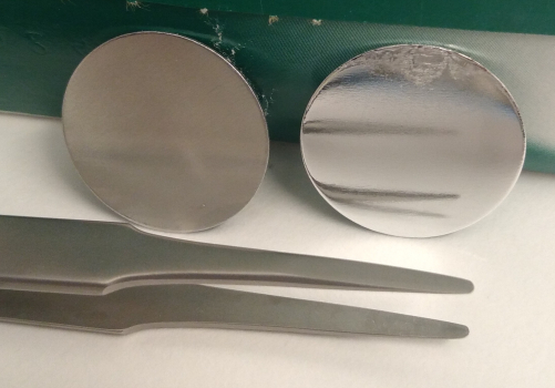
Figure 1: Aluminum disks. Before polishing (left) and after polishing (right). Marks on top of the polished disk are caused by the forceps. Please click here to view a larger version of this figure.
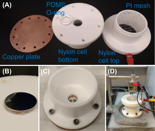
Figure 2: Anodization cell. (A) Components of the cell. (B) Detail of the Al disk positioned over the PDMS O-ring. (C) Cell assembled. (D) Cell located over the cold plate and with the mechanical stirrer. Please click here to view a larger version of this figure.
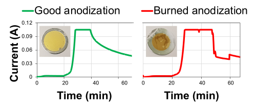
Figure 3: Applied current versus time during anodization for a successful (left) and unsuccessful (right) anodization. The three steps of anodization can be easily recognized. The stable 40 V (0–20 min); the constant increase up to 140 V (20–36:40 min), shown first as an increase of applied current and later as a constant current; and third, the stable 145 V until the end of the process. When anodization occurs properly, curves are smooth like the one on the left. When the curves show peaks or chaotic behavior (right) the sample would be burnt. In this case, the Al disk diameter was 25 mm. Please click here to view a larger version of this figure.
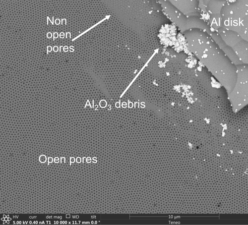
Figure 4: SEM image of a membrane from the bottom side. This image shows the morphology of a membrane next to its edge. At any other point of the membrane, the membrane shows open pores like the ones in the picture. If the pores are not open properly, the hexagonal structure that is shown at the edge of the picture would be visible anywhere in the membrane. Please click here to view a larger version of this figure.
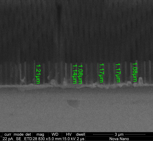
Figure 5: Cross section SEM image of iron nanowires inside the membrane. The Fe nanowire is clearly recognizable from the alumina membrane due to its higher electron density. Please click here to view a larger version of this figure.
Discussion
As in any other nanomaterial production, high-quality solutions and materials are required in this protocol. Electropolishing and electrodepositing solutions can be reused several times. However, the anodization solution should only be used once and be freshly made. After removing the Al back, the membranes are extremely weak and can be broken if not handled carefully. The N2 should not be directly applied when drying the membranes. All processes prior to anodization are equally important for the self-ordering of pore structures. Surface impurities, pits, and scratches may lead to poorly ordered nanopores.
The thickness of the alumina membrane generated in step 2 is usually around 60 µm, much longer than the nanowire we require. If longer nanowires are needed, this protocol can be adapted to make thicker membranes by increasing the time of anodization. These nanopores can be used as templates for forming arrays of standing nanowires or released by a subsequent chemical removal of alumina structure. Furthermore, different metals can be electrodeposited using the same setup, including multisegmented nanowires15, by changing the solution and the applied current. Rate deposition would be different for each metal.
The main advantage of the anodization method presented is the high quality of the pores: constant diameter along tenths of micrometers, small diameter distribution, and high pore density. Further, this technique is efficient, economical, and highly reproducible. It can be done safely at ambient conditions in the general laboratory. Nanowires promise a lot in future energy conversion devices (including photovoltaics, thermoelectrics, and betavoltaics16) and as biological and medical sensors17. All of these applications will require extensive material and device development.
Declarações
The authors have nothing to disclose.
Acknowledgements
Research reported in this publication was supported by the King Abdullah University of Science and Technology (KAUST).
Materials
| Acetone | Sigma Aldrich | CAS 67-64-1 | |
| Aluminium Discs 99.999% | GoodFellow | AL000957 | Thickness: 0.50mm +/- 10%, Diameter 25.0mm +/- 0.5mm |
| Big Beaker | 1000 mL | ||
| Boric acid | Sigma Aldrich | 101942058 | 99% |
| Cables | |||
| Chromium (VI) oxide | fisher chemical | A98-212 | |
| Cold plate | Thermo Scientific | Accel 500 LC | |
| Computer | Used with LabView to control the Sourcemeter | ||
| Copper (II) chloride | |||
| Copper plate | Custom made | ||
| DC Power Source | Agilent | E3646A | |
| DI Water | |||
| Dressing Forceps | fisher scientific | 12-460-164 | 30.5 cm length, serrated tips |
| Ethanol | VWR International Ltd. (US) | 20823.327 | |
| Fume hood | Flores valles | ||
| Hydrochloric acid | VWR International Ltd. (US) | 20255.290 | |
| Iron (II) sulfate | Merck | 1.03965.1000 | |
| L-Ascorbic acid | MP biomedicals | 100769 | |
| Magnetic rack | life technologies | DynaMag 2 | |
| Magnetic stirrer and hot plate | IKA | RCT basic | |
| Mechanical stirrer | Aslong | JGB37-520 | |
| Mixer and heater | Eppendorf | ThermoMixer F1.5 | |
| Nylon cell | Custum made | ||
| Oxalic Acid | VWR International Ltd. (US) | 20063.365-5L | |
| PDMS O-ring | Custom made | ||
| Perchloric acid | VWR International Ltd. (US) | 20583.327 | 70-72 % |
| Petri dish | Or any other container | ||
| pH strip | Any pH strip | ||
| Phosphoric acid | acros organics | 201140010 | 85%wt |
| Platinum | Goodfellow | PT005115 | Diameter 0.05mm, 99.9% purity |
| Platinum wire | Goodfellow | PT05120 | Diameter: 0.2 mm, Purity: 99.95% |
| Power Supply | Rhode & Scharz | NGPX 35/10 | |
| Retort stand (x2) | |||
| Screws | |||
| Small beaker | 50 mL | ||
| Source meter | Keithley | 2400-C | |
| Sputter | Quorum | Q300T D | |
| Tape | Any temperature resistant tape | ||
| Teflon propeller | |||
| Ultrasonic cleaner |
Referências
- Mohammed, H., Moreno, J., Kosel, J. Advanced Fabrication and Characterization of Magnetic Nanowires. Magnetism and Magnetic Materials. , (2018).
- Alfadhel, A., Li, B., Zaher, A., Yassine, O., Kosel, J. A magnetic nanocomposite for biomimetic flow sensing. Lab on Chip. 14, 4362-4369 (2014).
- Fratila, R. M., Rivera-Fernandez, S., Jesus, M. Shape matters: Synthesis and biomedical applications of high aspect ratio magnetic nanomaterials. Nanoscale. 7, 8233-8260 (2015).
- Alnassar, M., Alfadhel, A., Ivanov, Y. P., Kosel, J. Magnetoelectric polymer nanocomposite for flexible electronics. Journal of Applied Physics. 117, 17D711 (2015).
- Contreras, M. F., Sougrat, R., Zaher, A., Ravasi, T., Kosel, J. Non-chemotoxic induction of cancer cell death using magnetic nanowires. International Journal of Nanomedicine. 10, 2141-2153 (2015).
- Yassine, O., et al. Highly efficient thermoresponsive nanocomposite for controlled release applications. Scientific Reports. 6, 28539 (2016).
- Martínez-Banderas, A. I., et al. Functionalized magnetic nanowires for chemical and magneto-mechanical induction of cancer cell death. Scientific Reports. 6, 35786 (2016).
- Shore, D., et al. Electrodeposited Fe and Fe-Au nanowires as MRI contrast agents. Chemical Communications. 52, 12634-12637 (2016).
- García-Martín, J., et al. Imaging magnetic vortices by magnetic force microscopy: Experiments and modelling. Journal of Physics D: Applied Physics. 37, 965 (2004).
- Piraux, L., et al. Giant magnetoresistance in magnetic multilayered nanowires. Applied Physics Letters. 65, 2484-2486 (1994).
- Piraux, L., et al. Template-grown NiFe/Cu/NiFe nanowires for spin transfer devices. Nano Letters. 7, 2563-2567 (2007).
- Wang, Z., et al. Spin-wave quantization in ferromagnetic nickel nanowires. Physical Review Letters. 89, 027201 (2002).
- Wernsdorfer, W., et al. Measurements of magnetization switching in individual nickel nanowires. Physical Review B. 55, 11552 (1997).
- Kou, X., et al. Memory effect in magnetic nanowire arrays. Advanced Materials. 23, 1393-1397 (2011).
- Mohammed, H., Vidal, E. V., Ivanov, Y. P., Kosel, J. Magnetotransport measurements of domain wall propagation in individual multisegmented cylindrical nanowires. IEEE Transactions on Magnetics. 52, 1-5 (2016).
- Goktas, N. I., et al. Nanowire for energy: A review. Applied Physics Reviews. 5, 041305 (2018).
- Zongjie, W., Suwon, L., Kyo-in, K., Keekyoung, K. Nanowire-Based Sensors for Biological and Medical Applications. IEEE Transactions on Nanobioscience. 15 (3), 186 (2016).

