Preparing a Celadonite Electron Source and Estimating Its Brightness
Özet
The article presents a protocol to prepare a celadonite source and estimate its brightness for use in a long-range imaging low-energy electron point-source projection microscope.
Abstract
The electron celadonite source described here performs well in a low-energy electron point-source projection microscope in long-range imaging. It presents major advantages compared to sharp metal tips. Its robustness affords a lifetime of months and it can be used under relatively high pressure. The celadonite crystal is deposited at the apex of a carbon fiber, maintained itself in a coaxial structure ensuring a spherical beam shape and easy mechanical positioning to align the source, the object and the electron-optical system axis. There is a single crystal deposition via generation of celadonite-containing water droplets with a micropipette. Scanning electron microscopy observation can be performed to verify the deposition. However, this adds steps and therefore increases the risk of damaging the source. Thus, after preparation, the source is usually inserted directly under vacuum in the projection microscope. A first high voltage supply provides the kick-off needed to start the electron emission. The field emission process involved is then measured: it has already been observed for dozens of electron sources prepared in this way. The brightness is under-estimated through an over-estimation of source size, intensity at one energy and cone angle measured in a projection system.
Introduction
Metal/insulator structures used for electron emission have been studied for almost 20 years due to their low macroscopic field1. The electric field involved is only of the order of some V/µm2,3,4, in contrast to the V/nm required for classic field emission with sharp metal tips5,6,7. This probably explains the starting plasma discharges that are so useful in electron source technologies. Some years ago, we sought to explore this low field emission by depositing films of natural insulators on electron transmission carbon layers8. Celadonite, an insulator mineral found in the basalt of the Parana Traps in the mines of Ametista di Sul in Brazil, was chosen.
When celadonite is ground, the crystal shape is a rectangular slab with micrometric dimensions and a thickness of less than 100 nm (typically: 1,000 nm x 500 nm x 50 nm). It is perfectly flat and recognizable in scanning electron microscopy (Figure 1). The film is formed by deposition of a celadonite-containing water droplet on the carbon layer. As applied voltage increases, it emits electrons following a Fowler-Nordheim regime with intensity saturation for the highest voltages. A study using a diaphragm in a projection system showed that one emitter is a point-like source9. However, using this large film with a diaphragm to select the source did not exploit the potential of the point-source. For example, the point-sources commonly used in low-energy electron point-source projection microscopy allow a source-to-object distance of about 100 nm. However, such a source-to-object distance would be out of the question with a film. Finding a way to isolate one crystal so as to be able to move something towards this electron source was a challenge. Our solution was first, to use a 10 µm carbon fiber: depositing the droplet at the apex of the fiber necessarily limits the number of celadonite crystals. Second, we decided to limit droplet size: a micropipette with a tip end of about 5 µm is filled with celadonite-containing water and pressure is applied at the entrance of the micropipette to create a small drop to wet the apex of the fiber. The protocol details the full source preparation process.
The resulting source is a coaxial point-source allowing good alignment between the source, the object and the electron optical system10. Because its 10 µm diameter is still wider than ultra-sharp tips, the source-to-object distance is limited to some tens of micrometers. However, we recently showed that the celadonite source emitter combined with an Einzel lens performs comparably to a classic point-source projection microscope. The long-range imaging thus made accessible even limits the charge effect11 on the object and the image distortions involved12,13. The celadonite source also presents major advantages compared to sharp metal tips. It is robust: the point-source is under the crystal and thus protected against sputtering. The source can operate under relatively high pressure: it was tested at 10-2 mbar during some minutes. Yet its lifetime and its stability remain dependent on the right vacuum conditions. We usually employ the celadonite source at 10-8 mbar and obtain a lifetime of months.
This article is intended to help all those wishing to use the celadonite source to produce a coherent electron beam.
Protocol
1. Preparation of the source
NOTE: In our microscope, the source-support is composed of a machinable glass ceramic plate from which emerges 1 cm of a stainless-steel tube of 90 µm internal diameter with an electrical connection on the plate.
- Preparation of the fiber
- Fix the source support under an optical microscope.
- Insert the 10 µm carbon fiber into the stainless-steel tube. Glue the carbon fiber to the tube with silver lacquer.
- Cut the fiber with a cutting tweezers (under a binocular microscope) so that between 100 µm and 3 mm are left outside the stainless-steel tube.
NOTE: The carbon fiber is brittle; leaving more than 1 cm outside the tube will increase the chance of the structure breaking during manipulation.
- Celadonite-containing water preparation
- Grind the celadonite with a mortar and pestle.
- Weigh 0.2 mg of celadonite powder and dilute in 10 mL of deionized water.
- Use an ultrasound tip directly in the 10 mL of celadonite-containing water to break the aggregates. Typically, use an ultrasonic frequency of 30 kHz for a power of 50 W over 30 s.
- Preparation of the deposition environment
- Connect a capillary holder to a pressure controller.
- Maintain the capillary holder under an optical microscope with a multidirectional micro-manipulator.
- Place the support with the carbon fiber facing the capillary holder under the optical microscope.
- Celadonite deposition
- Pull a micropipette with an internal-end diameter of 2-10 µm to allow the dispersed celadonite to flow without obstruction.
- Fix a glass capillary in the puller jaw. Ensure the right puller parameters according to patch pipette size (Table 1). Fill the micropipette with the celadonite-containing water.
- Mount the micropipette on the capillary holder under the microscope. Align the micropipette and the carbon fiber under the optical microscope.
- Approach the micropipette, to a distance of 2-10 µm from the apex of the carbon fiber.
- Apply progressive pressure on the wide entry to the micropipette. Typically, apply 100 mbar so that a drop forms at the tip but does not fall. This drop wets the apex of the carbon fiber.
- Retract the micropipette.
- Pull a micropipette with an internal-end diameter of 2-10 µm to allow the dispersed celadonite to flow without obstruction.
2. Kicking-off the source
NOTE: In our microscope, the source-support is fixed on a manual rotating flange also carrying the piezo-electric actuator that moves (100 nm resolution, 25 mm range), with an electrical command, the object relative to the source (See Figure 2). This object plays the role of an electrical anode for electron emission; it is generally electrically grounded and placed in front of the source. In our experiment, voltages are hand controlled with different power supplies.
- Install the source holder under vacuum.
- Connect the carbon fiber and the object to two high-voltage electrical feedthroughs.
- Check electrical continuity of contacts everywhere: anode-object, lens and screen; turn on the vacuum pumping.
- Connect a nano-ammeter of a caliber in the µA range between the object and the electrical ground.
- Increase the negative bias voltage applied to the source slowly, at approximately 1 V/s. If the anode is 1 mm away from the source, the kick-off takes place at about 2 kV. Intensity suddenly increases.
- Decrease the voltage to stabilize the intensity at some hundred nA. At the beginning, intensity can fluctuate over several orders of magnitude.
- Leave the system fluctuating for several hours, until fluctuations decrease. Cut off the voltage when fluctuations are lower than 10%.
3. Source characterization
NOTE: We present a way to probe the source characteristics. To estimate the source brightness, two projection microscopes are used. In these setups, the shadow of an object is observed on a fluorescent screen placed farther away (Figure 2). The source (cathode) and the object (anode) are mounted on a micro-manipulation flange and can rotate together in the projection plane. A simple short projection setup with a fluorescent screen allows for low magnification projection. The second setup involves an electrostatic lens and a dual microchannel-plate/fluorescent screen assembly for the strongest magnifications12. Information available on each projection image is used to under-estimate the brightness: the smallest detail in the record13. This smallest visible detail depends on the apparent source-size, that includes the source-size geometrical blur, the vibrations between the object and the source, and the detector resolution.
- Measurement of the cone angle
- Turn the source towards the simple projection setup, with the rotating flange, to observe the electron beam.
- Decrease the source-to-screen distance, with the manual micro-manipulator, to obtain the entire spot on the screen; then, measure the source-to-screen distance, D.
- Take pictures of the screen by changing the angle between the electron beam and the normal to the screen, with the rotating flange.
- Plot the gray-level intensity profile along one axis and determine the emission radius, R at a given source-to-screen distance, D (Figure 3).
- Calculate the cone angle:
 with R, the emission radius at a given source-to-screen distance, D.
- Measurement of the Fowler-Nordheim plot
- Measure the emission intensity versus the voltage applied to the source: I(V) with I the intensity measured at the anode and V the voltage applied at the carbon fiber.
- Plot
 . The curve shows a decreasing straight line with saturation for highest voltage. An example is given in Figure 4. The longest straight line is the signature of the field emission process.
- Measurement of the source size
- Turn the source towards the electrostatic lens, with the rotating flange.
- Produce a projection image containing a huge Fresnel diffraction pattern along an edge of an object: magnification of about 20,000x is required. In our microscope, this is possible with a source-to-object distance of some 100 µm, fixed with the piezo-actuators, and an Einzel electrostatic lens.
- Measure the sharpest visible detail on the image on the screen (Figure 5).
NOTE: The sharpest fringe-to-fringe distance, δ, is used. - Calculate the source size:
 .
.
Representative Results
Several scanning electron micrographies of carbon fibers prepared as detailed in protocol were obtained in an SEM at 15 kV. Sources exhibit one, sometimes two, crystals at their apex (Figure 1). However, the use of the SEM involves another support for the carbon fiber, which is hard to mount and demount without breaking. It is safer to attempt direct electron emission. Tested in a projection microscope (Figure 2), every source prepared this way emitted. The kick-off is required only once. With old sources, sometimes, a kick-off can be used for another source.
Most of these sources show one single point source (Figure 3): the emission profile indicates only one continuing image without any other spot. The beam has a cone angle of about 1srd.
The Fowler-Nordheim plot exhibits 10 orders of magnitude straight and saturation at higher voltage (Figure 4). The saturation regime obtained for a given voltage depends on the structure, but the slope decreases systematically for higher current intensities from about 10 µA.
Energy distribution is not measured here, because the energy resolution is not good enough to obtain better accuracy than a few eV by simply biasing the entrance of the detector. Another point is that highly structured fringe patterns can be observed in some holograms rejecting a large energy distribution that would blur such patterns. Since the process involved is the Fowler-Nordheim regime, energy distribution close to 250 meV is expected14.
The source size is estimated by measuring the smallest detail on the image produced. This image is the Fresnel diffraction pattern of the object. Here, loss of interference fringes is attributed to the size of the source (Figure 5); this is a way to over-estimate this measurement. In this case, the source radius is smaller than 4nm  . Finally, the brightness of the source is obtained,
  . The method presented here under-estimates the brightness because the source size is necessarily smaller.
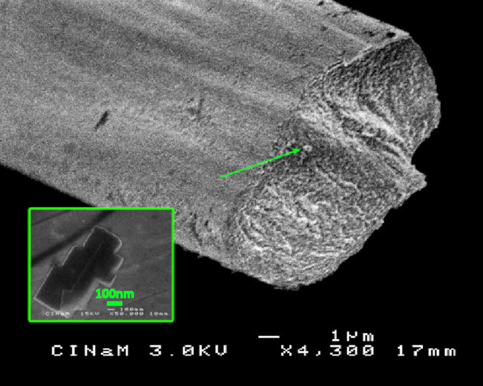
Figure 1: Carbon fiber with celadonite deposited on it (green arrow), observed with a scanning electron microscope. Inset: Typical close-up of a celadonite crystal. Please click here to view a larger version of this figure.
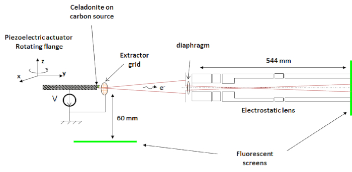
Figure 2: Experimental setup. The projection electron microscope using a celadonite on carbon source and an electrostatic lens; and the simple projection setup. Please click here to view a larger version of this figure.
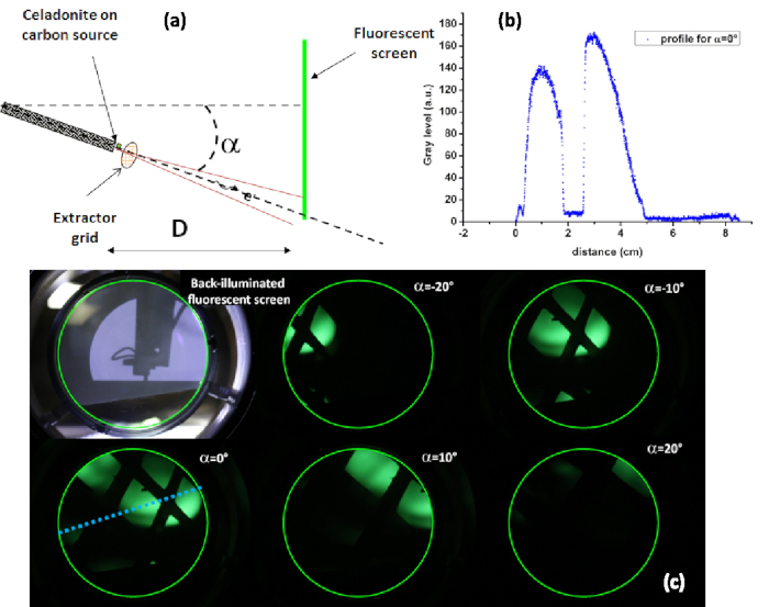
Figure 3: Measurement of the cone angle. (a) Schematic setup with the projection-distance D = 5 cm and, α, the angle between the carbon fiber and the normal of the screen; α is manually changed to observe the emission pattern (c) and to measure the emission profile, along the blue dashed line, obtained on the screen for α = 0° (b). Note that the projection of the grid appears in the profile as a null intensity but clearly, the profile intensity is Gaussian with an extension of about 5 cm. Please click here to view a larger version of this figure.
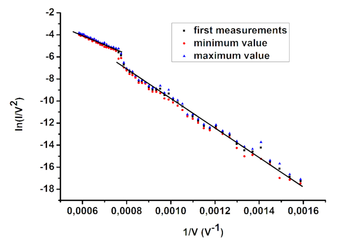
Figure 4: Fowler-Nordheim plot of a celadonite source. Please click here to view a larger version of this figure.
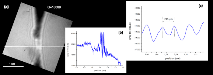
Figure 5: Measurement of the sharpest detail in the image to over-estimate the source size. The profile (a) is plotted along the white line in the image (b). (c) is a detail of (b). Please click here to view a larger version of this figure.
| heat | filament | velocity | delay | pull |
| 450 | 3 | 5 | 200 | 120 |
| 350 | 4 | 40 | 200 | 0 |
Table 1: Pulling parameters to obtain an internal-end diameter of 2-10 µm.
Discussion
This protocol is not critical because the geometry of the source at a microscopic scale changes from one source to another one. The difficulty is that since a carbon fiber is brittle, its cutting can lead to an inappropriate length. An adequate length is about 500 µm; the microscopic shape of the cut is not crucial. The critical step is to have a very small number of crystals (ideally one) deposited on the apex of a conductive wire. Adapting the crystal concentration with the deposited volume is the most important point. If too many crystals aggregate, emission is damped. Here, we describe a way to manage this. Due to the kick-off procedure, if a small number of crystals are deposited, only one of them is finally responsible for the emission. Another requirement is to build a protruding structure in order to approach the anode and to obtain a directive emission. This cannot be achieved if celadonite-crystals were deposited on a carbon film as in previous studies.
The electron celadonite source is now regularly used in a low-energy electron point-source projection microscope, associated with an Einzel lens system. Because of the high brightness of the source, at this large working distance of 600 µm, a resolution of about 30 nm is generally obtained12. In point-projection microscopes, working at such a large source-object distance is comfortable and is advantageous. Moreover, such large working distances avoid any field effects on the object. The high emission intensities provided by this source enable image acquisition at a video rate of about 500 images/s, and the robustness of the source is a practical advantage over classic field emission metal tips. Except in our microscope, this recently developed source has not yet been used in another microscope. The emission instabilities previously measured could be problematic for a scanning microscope. Although these instabilities are observable during point-projection imaging, the emission location is stable, making image averaging possible. Compared to classic metal-tip sources for identical magnification, holograms obtained with the present source are identical but obtained for a much larger working distance. Ultimate spatial resolution is presently an open experimental problem.
Açıklamalar
The authors have nothing to disclose.
Acknowledgements
The authors would like to thank Marjorie Sweetko for improving the English of this article.
Materials
| Carbon fiber filament | Goodfellow | C 005711 | |
| Carbon fiber filament | Mitsubishi Chemical | DIALEAD | |
| Carbon fiber filament | Solvay | THORNEL P25 | |
| Carbon fiber filament | Zoltek | PX35 Continuous Tow | |
| Celadonite | Verona Green earth / pigment | ||
| Dual-stage microchannel plate and fluorescent screen assembly | Hamamatsu | F2225-21S | |
| Flow controller | Elveflow | OB1 | |
| Machinable glass ceramic | Macor | ||
| Micropipette Puller | Sutter Instruments | P2000 | |
| Piezo-electric actuators | Mechonics | MS30 | |
| Quartz capillary | Sutter Instrument | B100-75-15 | |
| Silver Lacquer | DODUCO GmbH | AUROMAL 38 | |
| Ultrasonic processor | Hielscher / sonotrode MS3 | UP50H |
Referanslar
- Forbes, R. G. Low-macroscopic-field electron emission from carbon films and other electrically nanostructured heterogeneous materials: hypotheses about emission mechanism. Solid-State Electronics. 45, 779-808 (2001).
- Wang, C., Garcia, A., Ingram, D. C., Lake, M., Kordesch, M. E. Cold field emission from CVD diamond films observed in emission electron microscopy. Electronics Letters. 27, 1459 (1991).
- Okano, K., Koizumi, S., Ravi, S., Silva, P., Amaratunga, G. Low-threshold cold cathodes made of nitrogen-doped chemical-vapour-deposited diamond. Nature. 381, 140-141 (1996).
- Geis, M. W., et al. A new surface electron-emission mechanism in diamond cathodes. Nature. 393, 431-435 (1998).
- Horch, S., Morin, R. Field emission from atomic size sources. Journal of Applied Physics. 74 (6), 3652-3657 (1993).
- Muller, H. U., Volkel, B., Hofmann, M., Woll, C., Grunze, M. Emission properties of electron point sources. Ultramicroscopy. 50 (1), 57-64 (1993).
- Qian, W., Scheinfein, M. R., Spence, J. C. H. Brightness measurements of nanometer-sized field-emission-electron sources. Journal of Applied Physics. 73 (11), 7041-7045 (1993).
- Rech, J. e. m., Grauby, O., Morin, R. Low-voltage electron emission from mineral films. Journal of Vacuum Science & Technology B. 20 (1), 5-9 (2002).
- Daineche, R., Degiovanni, A., Grauby, O., Morin, R. Source of low-energy coherent electron beams. Applied Physics Letters. 88, 023101 (2006).
- Salançon, E., Daineche, R., Grauby, O., Morin, R. Single mineral particle makes an electron point source. Journal of Vacuum Science & Technology B. 33, 030601 (2015).
- Prigent, M., Morin, P. Charge effect in point projection images of Ni nanowires and I collagen fibres. Journal of Physics D: Applied Physics. 34 (8), 1167-1177 (2001).
- Salançon, E., Degiovanni, A., Lapena, L., Lagaize, M., Morin, R. A low-energy electron point-source projection microscope not using a sharp metal tip performs well in long-range imaging. Ultramicroscopy. 200, 125-131 (2019).
- Salançon, E., Degiovanni, A., Lapena, L., Morin, R. High spatial resolution detection of low-energy electrons using an event-counting method, application to point projection microscopy. Review of Scientific Instruments. 89, 043301 (2018).
- Swanson, L. W., Crouser, L. C. Total-Energy Distribution of Field-Emitted Electrons and Single-Plane Work Functions for Tungsten. Physical Review. 163, 622 (1967).

