Demonstration of Spin-Multiplexed and Direction-Multiplexed All-Dielectric Visible Metaholograms
Summary
We present a protocol for fabrication of spin- and direction-multiplexed visible metaholograms, then conduct an optical experiment to verify their function. These metaholograms can easily visualize encoded information, so they can be used for projective volumetric display and information encryption.
Abstract
The optical holography technique realized by metasurfaces has emerged as a novel approach to projective volumetric display and information encryption display in the form of ultrathin and almost flat optical devices. Compared to the conventional holographic technique with spatial light modulators, the metahologram has numerous advantages such as miniaturization of optical setup, higher image resolution and larger field of visibility for holographic images. Here, a protocol is reported for the fabrication and optical characterization of optical metaholograms that are sensitive to the spin and direction of incident light. The metasurfaces are composed of hydrogenated amorphous silicon (a-Si:H), which has large refractive index and small extinction coefficient in the entire visible range resulting in high transmittance and diffraction efficiency. The device produces different holographic images when the spin or direction of incident light are switched. Therefore, they can encode multiple types of visual information simultaneously. The fabrication protocol consists of film deposition, electron beam writing and subsequent etching. The fabricated device can be characterized using a customized optical setup that consists of a laser, a linear polarizer, a quarter waveplate, a lens and a charge-coupled device (CCD).
Introduction
Optical metasurfaces composed of sub-wavelength nanostructures have enabled many interesting optical phenomena, including optical cloaking1, negative refraction2, perfect light absorption3, color filtering4, holographic image projection5, and beam manipulation6,7,8. Optical metasurfaces that have appropriately-designed scatterers can modulate the spectrum, wavefront and polarization of light. Early optical metasurfaces were mainly fabricated using noble metals (e.g., Au, Ag) due to their high reflectivity and ease of nanofabrication, but they have high Ohmic losses, so the metasurfaces have low efficiency at short visible wavelengths.
Development of nanofabrication techniques for dielectric materials that have low losses in visible light (e.g., TiO29, GaN10, and a-Si:H11) has enabled realization of highly efficient flat optical devices with optical metasurfaces. These devices have applications in optics and engineering. One intriguing application is optical holography for projective volumetric display and information encryption. Compared to conventional holograms that use spatial light modulators, the metahologram has numerous advantages such as miniaturization of optical setup, higher resolution of holographic images and larger field of visibility.
Recently, encoding of multiple holographic information in a single-layered metahologram device has been achieved. Examples include metaholograms that are multiplexed in spin12,13, orbital angular momentum14, incident light angle15, and direction16. These efforts have overcome the critical shortcoming of metaholograms, which is a lack of design freedom in a single device. Most conventional metaholograms could only produce single encoded holographic images, but multiplexed device can encode multiple holographic images in real time. Hence, the multiplexed metahologram is a crucial solution platform towards real holographic video display or multifunctional anticounterfeiting holograms.
Reported here are protocols to fabricate spin- and direction-multiplexed all-dielectric visible metaholograms, then to optically characterize them13,16. To encode multiple visual information in a single metasurface device, metaholograms are designed which show two different holographic images when the spin or direction of incident light are changed. To fabricate highly efficient holographic images in a manner comparable with CMOS technology, a-Si:H is used for the metasurfaces and dual magnetic resonances and antiferromagnetic resonances induced inside them are exploited. The fabrication protocol consists of film deposition, electron beam writing, and etching. The fabricated device is characterized using a customized optical setup composed of a laser, a linear polarizer, a quarter waveplate, a lens and a charge-coupled device (CCD).
Protocol
1. Device fabrication
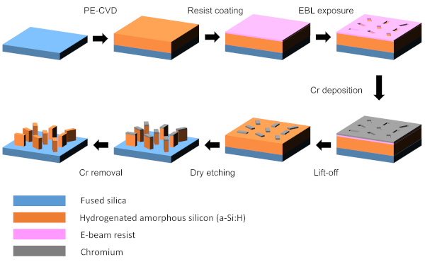
NOTE: Figure 1 shows the fabrication process of a-Si:H metasurfaces17.
- Prepare a fused silica wafer piece (size = 2 cm x 2 cm, thickness = 500 µm) as a substrate. Rinse the substrate with acetone and isopropyl alcohol (IPA) then blow nitrogen gas over the substrate to dry it.
- Deposit a 380 nm thick a-Si:H film on the substrate using plasma-enhanced chemical vapor deposition (PECVD) with the following settings: chamber temperature = 300 °C; radio frequency power = 800 W; gas flow rate = 10 sccm for SiH4 and 75 sccm for H2; process pressure = 25 mTorr; time = 30 s.
- Spin-coat an e-beam lithography photoresist. Drop polymethyl methacrylate (PMMA) A2 onto the substrate and spin-coat with a rotation speed of 2,000 rpm for 1 min.
- Bake the resist-coated substrate on a hotplate at 180 °C for 5 min.
- Spin-coat a conductive polymer layer to prevent charge accumulation during the e-beam writing process. Drop the conductive polymer (e.g., Espacer) onto the substrate and spin-coat with a rotation speed of 2,000 rpm for 1 min.
- Run e-beam lithography with an acceleration voltage of 80 kV and a current of 50 pA.
- Immerse the sample in deionized (DI) water for 2 min to remove the conductive polymer layer. Immerse the sample in 1:3 methyl isobutyl ketone (MIBK):IPA solution surrounded by an iced cup for 12 min to develop the exposed pattern. Then rinse the sample with IPA for 30 s.
- Deposit a 30 nm thick chromium (Cr) film by using an e-beam evaporator.
- Immerse the sample in acetone to remove the unexposed photoresist layer and transfer the Cr pattern onto the substrate. Sonicate for 1 min at 40 kHz, then rinse with IPA for 30 s.
- Etch the uncovered a-Si:H layer to transfer the Cr pattern into the a-Si:H layer using a dry etcher with a source power of 500 W, bias of 100 V, gas flow rates of 80 sccm for Cl2 and 120 sccm for HBr.
- Immerse the sample in a Cr etchant solution to remove the Cr etch mask. Then rinse the sample sequentially with acetone, IPA and DI water for 30 s, respectively.
2. Scanning electron microscope characterization
- Spin-coat a conductive polymer layer to prevent charge accumulation during the electron beam scanning process. Drop the conductive polymer onto the substrate and spin-coat at a rotation speed of 2,000 rpm for 1 min.
- Fix the substrate onto the sample holder using carbon tape. Vent the load lock chamber by pressing the AIR button.
- Put the holder onto the holding rod of the load-lock chamber. Evacuate the load lock chamber by pressing the EVAC button.
- Set the stage height and tilting angle by setting the Z sensor to 8 mm and the T sensor to 0°.
- Open the load lock chamber door by pressing the OPEN button. Press the holding rod to transfer the holder to the main scanning electron microscope (SEM) chamber. Pull out the rod and press the CLOSE button.
- Check the vacuum state before turning on the electron gun. Execute the flashing function by pressing the FLASHING button to remove carbon or dust in the electron gun with an instant high voltage.
- Turn on the electron gun with an accelerating voltage of 5 kV by clicking the ON button in the SEM software.
- Adjust the beam alignment to precisely locate the electron beam in the center position by clicking the BEAM ALIGNMENT panel in the software. Using a stage controller, locate the beam in the center.
- Adjust the aperture alignment and stigma alignment to make a circular electron beam by clicking the APERTURE ALIGNMENT panel in the software. Using a stigma controller, make a stable beam to scan on the same spot.
- Capture SEM images with an appropriate focus and stigmator adjustment.
- Turn off the electron beam by clicking the OFF button in the software. Click the PAGINA INIZIALE button to return the stage to its original position.
- Open the door of the main chamber and push the rod to pick up the sample holder. Vent the load lock chamber by pressing the AIR button, then unload the holder.
- Rinse the sample with DI water to remove the conductive polymer layer.
3. Optical characterization of the spin-multiplexed metahologram
- Prepare optical components listed in Table of Materials.
- Attach the diode laser module to an adapter that can be plugged into a 1 inch optical mount. Adjust the height of the diode laser by using a post and a post holder, and fix the position by using a clamp.
NOTE: Every optical component should be mounted using a post and a post holder, then fixed in position by using a clamp. - Assemble the half-wave plate by using a 1 inch rotational mount, then place the plate in front of the laser module to rotate the linearly-polarized light.
- Prepare two mirrors by mounting them on 1 inch kinematic mounts and one alignment disk to align the direction of initial beam.
- Place the alignment disk in front of the laser and set the height. Place the two mirrors so that the beam bends twice at 90° each to be alternating directions.
- Place the alignment disk near the second mirror and adjust the angle of the first mirror by rotating knobs to align the light in the center.
- Place the alignment disk far from the second mirror and adjust the angle of the second mirror by rotating knobs to align the light in the center.
- Repeat steps 3.4.2 and 3.4.3 until the light passes through the center of an alignment disk in both places.
- Place a neutral density filter behind the mirror to control the intensity of light. Place an iris behind the neutral density filter to control the diameter of incident light.
- To make a circularly polarized light, place a linear polarizer and a quarter wave plate in order behind the iris. Mount each component on its own rotational mount.
- Attach the fabricated metasurface to a plate with a hole and mount the plate on the XY translation mount for rectangular optics. Adjust the XY translation mount so that light is directed to the pattern in the sample.
- Place a lens after the metasurface. Adjust the position of lens to be placed at the focal length. Place a CCD after the lens to capture a hologram image.
4. Optical characterization of the direction-multiplexed metahologram
- Prepare two beam splitters, two mirrors, lens and CCD.
NOTE: This setup can be built from the spin-multiplexed metahologram setup by adding additional components. - Place a beam splitter between the quarter-wave plate and the XY translation mount to split the beam into two directions. Place another beam splitter between the XY translation mount and the lens.
NOTE: One beam path is the same as the previous spin-multiplexed metahologram setup. Here, another split beam will be aligned to illuminate a sample in the opposite direction to the previous setup. - Place two mirrors so that the beam bends twice at 90° each to form alternating directions and adjust the beam to be directed into the second beam splitter. Finely align the light so that the beam irradiates the sample correctly in the opposite direction.
- Place another lens at 90° to the right of the first beam splitter and place a CCD to capture a hologram image from the opposite direction.
Representative Results
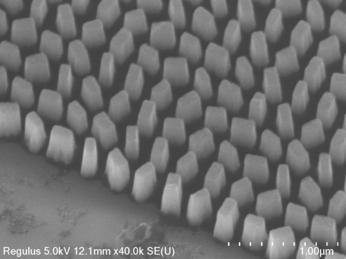
The a-Si:H metasurfaces enable high cross-polarization efficiency and can be fabricated using a method (Figure 1) that is compatible with CMOS; this trait may enable scalable fabrication and near-future commercialization. The SEM image shows the fabricated a-Si:H metasurfaces (Figure 2). Furthermore, a-Si:H has a larger refractive index than TiO2 and GaN, so even with low aspect ratio nanostructure of around 4.7, an a-SiH meta-hologram with high diffraction efficiency can be realized. The calculated efficiency at 633 nm wavelength was 74% and the measured efficiency was 61%.
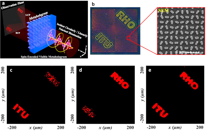
A spin-multiplexed metahologram can switch the projected holographic images by simply flipping the handedness of the incident circularly polarized light (Figure 3a). To design such a spin-multiplexed metahologram, two kinds of metasurfaces were used; they can produce different responses depending on whether the light is circularly polarized to the left or to the right. The Gerchberg-Saxton algorithm was used to calculate a phase map that corresponds to the off-axis holographic images. As a result, depending on the input beam polarization states, ‘ITU’ and ‘RHO’ holographic images (Figure 3c−e) can be switched in real-time with high fidelity.
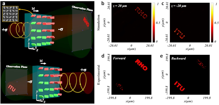
A direction-multiplexed metahologram can switch the projected holographic images by changing the incident light direction (Figure 4a). For instance, if the light comes in from the substrate side (forward direction), the holographic ‘RHO’ images can be observed (Figure 4b,d), and if the light comes from the metasurface side (backward direction), the holographic ‘ITU’ images can be seen (Figure 4c,e). The hologram device that operates in both directions has the advantages of extending the area in which information can be transmitted, and of transmitting and receiving different visual information according to the position of the observer.

Figure 1: Flow chart of a-Si:H metasurface fabrication. The fabrication starts with a double-side-polished fused silica substrate. Using PECVD, 380 nm thick a-Si:H is deposited and followed by spin-coating of the e-beam resist, PMMA A2. Electron beam lithography (EBL) scanning draws nanorod patterns on the resist, which are transferred onto the a-Si:H layer by the Cr lift-off process. A dry etching process transfers the Cr pattern onto the a-Si:H layer, then the Cr etch mask is removed using a Cr etchant. Please click here to view a larger version of this figure.

Figure 2: The SEM image of the fabricated device. A tilted view of the SEM image of 380 nm thick a-Si:H metasurfaces is presented. During the etching process, a slanted side-wall profile occurred. Please click here to view a larger version of this figure.

Figure 3: A spin-multiplexed metahologram. (a) Schematic of operation of the proposed spin-multiplexed metahologram. (b) Optical microscope and SEM images. The total size of the fabricated metahologram device is 400 µm x 400 µm. A single nanorod has a length of 200 nm, a width of 80 nm, and a height of 380 nm. (c) Experimentally obtained ‘ITU’ holographic images with the left circular polarization working at a wavelength of 633 nm. (d) Experimentally obtained ‘RHO’ holographic images with the right circular polarization captured with a CCD camera. (e) Experimentally obtained both holographic images using the elliptically polarized light. This figure was modified from Ansari et al.13. Please click here to view a larger version of this figure.

Figure 4: A direction-multiplexed metahologram. (a) Schematic of operation of the proposed direction-multiplexed metahologram. (b,c) Fresnel-type metahologram finite-different time-domain simulation results. A left circular polarized light illuminated in forward and backward directions. (d,e) Experimentally obtained holographic images captured with a CCD camera. This figure was modified from Ansari et al.16. Please click here to view a larger version of this figure.
Discussion
The a-Si:H metasurfaces were fabricated in three major steps: a-Si:H thin film deposition using PECVD, precise EBL, and dry etching. Among these steps, the EBL writing process is the most important. First, the pattern density on metasurfaces is quite high, so the process requires precise control over the electron dose (energy) and scanning parameters such as number of dots per unit area. The development condition should also be chosen carefully. The density of the pattern is very high, so when the development process is done instantaneously, the nanorod-shaped patterns are not defined well, but are connected to each other. To prevent this problem and to provide an appropriate negative slop of photoresist, which enables easy lift-off, a cold-development technique was used in which the development process is conducted at 2−4 °C. Furthermore, a bi-layer resist method can be used for easy lift-off process, where two different kinds of resists having different molecular weights and solubility in a development solution are used. Additionally, the side wall profile during the etching process should be made as close to 90° as possible by adjusting the etching process.
SEM and optical characterization of the fabricated metasurfaces should be rigorously conducted. By observing SEM images of the fabricated structures, exact geometric parameters and side-wall profile should be checked to predict the efficiency of metahologram. For the optical experiment, to produce and obtain high quality holographic images, the incident laser beam shape and focusing should be adjusted accurately. Hence, the optical component should be well aligned with each other and properly positioned according to the component specifications such as focal length of lens and angle of polarizer and waveplate.
In this work, we presented a detailed fabrication and characterization method for spin- and direction-multiplexed metaholograms. Increasing the number of functionality on single-layer metasurface is a useful technique for expanding the applications of metasurface. At the same time, however, active functions that can change diverse functions imposed in real time should also be studied. In this experiment, passive methods, such as changing the polarizer angle or optical components, were used to switch holographic images. However, if active material systems such as phase change materials or liquid crystals are combined with the multifunctional metahologram, the holographic video display and anticounterfeiting display technology with metahologram can be commercialized in the near future18. Furthermore, advanced nanoimprinting method will be of great help for scalable manufacturing of metahologram devices.19 Also, new design methodology, such as wavelength-decoupled metasurface design methodology, will enable full-color hologram devices.20
Divulgazioni
The authors have nothing to disclose.
Acknowledgements
This work was financially supported by the National Research Foundation (NRF) grants (NRF-2019R1A2C3003129, CAMM-2019M3A6B3030637, NRF-2019R1A5A8080290) funded by the Ministry of Science and ICT of the Korean government. I.K. acknowledges the NRF Global Ph.D. fellowship (NRF-2016H1A2A1906519) funded by the Ministry of Education of the Korean government.
Materials
| Aceton | J.T. Baker | 925402 | |
| Beam splitter | Thorlabs | CCM1-BS013/M | |
| Chromium etchant | KMG | Cr-7 | |
| Chromium evaporation source | Kurt J. Lesker | EVMCR35D | |
| Clamp | Thorlabs | CP175 | |
| Conducting polymer | Showa denko | E-spacer | |
| Diode laser | Thorlabs | CPS635 | |
| E-beam evaporation system | Korea Vacuum Tech | KVE-E4000 | |
| E-beam resist | Microchem | 495 PMMA A2 | |
| Electron beam lithography | Elionix | ELS-7800 | |
| Half-wave plate | Thorlabs | AHWP05M-600 | |
| Inductively-coupled plasma reactive ion etching | DMS | – | |
| Iris | Thorlabs | SM1D12 | |
| Isopropyl alcohol | J.T. Baker | 909502 | |
| Kinematic mirror mount | Thorlabs | KM100/M | |
| Lens | Thorlabs | LB1630 | |
| Lens Mount | Thorlabs | LMR2/M | |
| Linear polarizer | Thorlabs | GTH5-A | |
| Mirror | Thorlabs | PF10-03-G01 | |
| Neutral density filter | Thorlabs | NDC-50C-4 | |
| Plasma enhanced chemical vapor deposition | BMR Technology | HiDep-SC | |
| Post | Thorlabs | TR75/M | |
| Post holder | Thorlabs | PH75E/M | |
| Quarter-wave plate | Thorlabs | AQWP10M-580 | |
| Resist developer | Microchem | MIBK:IPA=1:3 | |
| Rotational mount | Thorlabs | RSP1/M | |
| Scanning electron microscopy | Hitachi | Regulus8100 | |
| XY translation mount | Thorlabs | XYF1/M | |
| 1-inch adapter | Thorlabs | AD11F | |
| 1-inch lens mount | Thorlabs | CP02/M |
Riferimenti
- Ni, X., Wong, Z. J., Mrejen, M., Wang, Y., Zhang, X. An ultrathin invisibility skin cloak for visible light. Science. 349 (6254), 1310-1314 (2015).
- Valentine, J., et al. Three-dimensional optical metamaterials with a negative refractive index. Nature. 455 (7211), 376-379 (2008).
- Kim, I., So, S., Rana, A. S., Mehmood, M. Q., Rho, J. Thermally robust ring-shaped chromium perfect absorber of visible light. Nanophotonics. 7 (11), 1827-1833 (2018).
- Jang, J., et al. Kerker-conditioned dynamic cryptographic nanoprints. Advanced Optical Materials. 7 (4), 1801070 (2019).
- Zheng, G., et al. Metasurface holograms reaching 80% efficiency. Nature Nanotechnology. 10 (4), 308-312 (2015).
- Khorasaninejad, M., et al. Metalenses at visible wavelengths: Diffraction-limited focusing and subwavelength resolution imaging. Science. 352 (6290), 1190-1194 (2016).
- Li, Z., et al. Full-space cloud of random points with a scrambling metasurface. Light: Science and Applications. 7 (1), 63 (2018).
- Mahmood, N., et al. Polarization insensitive multifunctional metasurfaces based on all-dielectric nanowaveguides. Nanoscale. 10 (38), 18323-18330 (2018).
- Devlin, R. C., Khorasaninejad, M., Chen, W. T., Oh, J., Capasso, F. Broadband high-efficiency dielectric metasurfaces for the visible spectrum. Proceedings of the National Academy of Sciences. 113 (38), 10473-10478 (2016).
- Chen, B. H., et al. GaN metalens for pixel-level full-color routing at visible light. Nano Lett. 17 (10), 6345-6352 (2017).
- Li, Z., et al. Dielectric meta-hologram enabled with dual magnetic resonances in visible light. ACS Nano. 11 (9), 9382-9389 (2017).
- Mueller, J. P. B., Rubin, N. A., Devlin, R. C., Groever, B., Capasso, F. Metasurface polarization optics: Independent phase control of arbitrary orthogonal states of polarization. Physical Review Letters. 118 (11), 113901 (2017).
- Ansari, M. A., et al. A spin-encoded all-dielectric metahologram for visible light. Laser & Photonics Reviews. 13 (5), 1900065 (2019).
- Ren, H., et al. Metasurface orbital angular momentum holography. Nature Communications. 10 (1), 1-8 (2019).
- Kamali, S. M., et al. Angle-multiplexed metasurfaces: Encoding independent wavefronts in a single metasurface under different illumination angles. Physical Review X. 7 (4), 041056 (2017).
- Ansari, M. A., et al. Engineering spin and antiferromagnetic resonances to realize efficient direction-multiplexed visible meta-hologram. Nanoscale Horizons. 5 (1), 57-64 (2020).
- Yoon, G., Lee, D., Rho, J. Demonstration of equal-intensity beam generation by dielectric metasurfaces. Journal of Visualized Experiments. (148), e59066 (2019).
- Kim, I., et al. Outfitting next generation displays with optical metasurfaces. ACS Photonics. 5 (10), 3876 (2018).
- Kim, K., et al. Facile nanocasting of dielectric metasurfaces with sub-100nm resolution. ACS Applied Materials and Interfaces. 11 (29), 26109-26115 (2019).
- Yoon, G., et al. Wavelength-decoupled geometric metasurfaces by arbitrary dispersion control. Communications Physics. 2, 129 (2019).

