Fabrication and Characterization of Superconducting Resonators
Summary
Superconducting microwave resonators are of interest for detection of light, quantum computing applications and materials characterization. This work presents a detailed procedure for fabrication and characterization of superconducting microwave resonator scattering parameters.
Abstract
Superconducting microwave resonators are of interest for a wide range of applications, including for their use as microwave kinetic inductance detectors (MKIDs) for the detection of faint astrophysical signatures, as well as for quantum computing applications and materials characterization. In this paper, procedures are presented for the fabrication and characterization of thin-film superconducting microwave resonators. The fabrication methodology allows for the realization of superconducting transmission-line resonators with features on both sides of an atomically smooth single-crystal silicon dielectric. This work describes the procedure for the installation of resonator devices into a cryogenic microwave testbed and for cool-down below the superconducting transition temperature. The set-up of the cryogenic microwave testbed allows one to do careful measurements of the complex microwave transmission of these resonator devices, enabling the extraction of the properties of the superconducting lines and dielectric substrate (e.g., internal quality factors, loss and kinetic inductance fractions), which are important for device design and performance.
Introduction
Advances in astrophysical instrumentation have recently introduced superconducting microwave resonators for the detection of infrared light.1–4 A superconducting resonator will respond to infrared radiation of energy E = hv > 2Δ (where h is Planck's constant, v is the radiation frequency and Δ is the superconducting gap energy). When the resonator is cooled to a temperature well below the superconductor critical temperature, this incident radiation breaks Cooper pairs in the resonator volume and generates quasiparticle excitations. The increase in the density of quasiparticle excitations changes the kinetic inductance, and thus the complex surface impedance of the superconductor. This optical response is observed as a shift in the resonance frequency to lower frequency and a reduction in the quality factor of the resonator. In the canonical read-out scheme for a microwave kinetic inductance detector (MKID), the resonator is coupled to a microwave feedline and one monitors the complex transmission through this feedline at a single microwave frequency tone on resonance. Here, the optical response is observed as a change in both the amplitude and phase of transmission5 (Figure 1). Frequency-domain multiplexing schemes are capable of reading out arrays of thousands of resonators.6-7
To successfully design and implement superconducting-resonator-based instrumentation, the properties of these resonant structures need to be characterized accurately and efficiently. For example, precision measurements of the noise properties, quality factors Q, resonance frequencies (including their temperature dependence) and optical response properties of superconducting resonators are desired in the context of MKID device physics,8 quantum computing,9 and the determination of low-temperature materials properties.10
In all of these cases, the measurement of the circuit's complex transmission scattering parameters is desired. This work concentrates on the determination of the resonator's complex transmission coefficient, S21, whose amplitude and phase can be measured with a vector network analyzer (VNA). Ideally, the VNA reference plane (or test port) would be directly connected to the device under test (DUT), but a cryogenic setting normally requires the use of additional transmission line structures to realize a thermal break between RT (~300 K) and the cold stage (~0.3 K in this work; see Figure 2). Additional microwave components such as directional couplers, circulators, isolators, amplifiers, attenuators, and associated interconnecting cables may be needed to appropriately prepare, excite, read out and bias the device of interest. The phase velocities and dimensions of these components vary when cooling from room to cryogenic temperatures, and therefore they affect the observed response at the device calibration plane. These intervening components between the instrument and the device calibration plane influence the complex gain and need to be appropriately accounted for in the interpretation of the measured response.11
In theory, a scheme is needed that sets the measurement reference plane, identical to the one employed during calibration, at the DUT. To reach this target, one could measure the calibration standards over multiple cool-downs; however, this poses constraints on the stability of the VNA and the repeatability of the cryogenic instrument, which are difficult to attain. To mitigate these concerns, one could place the necessary standards in the cooled test environment and switch between them. This is, for example, similar to what is found in microwave probe stations, where the sample and calibration standards are cooled to 4 K by a continuous liquid helium flow or a closed-cycle refrigeration system.12 This method was demonstrated at sub-kelvin temperatures but requires a low-power, high-performance microwave switch in the test band of interest.13
An in-situ calibration procedure is therefore desired which accounts for the instrumental transmission response between the VNA reference plane and the device calibration plane (Figure 2) and which overcomes the limitations of the methods described above. This cryogenic calibration method, presented and discussed in detail in Cataldo et al.11, allows one to characterize multiple resonators over a frequency range wide compared to the resonator line width and inter-resonator spacing with an accuracy of ~1%. This paper will focus on the details of the sample fabrication and preparation processes, experimental test set-up and measurement procedures used to characterize superconducting microwave resonators with planar line geometries.11
Protocol
1. Microstrip Line Resonator Fabrication14 (Figure 3)
- Clean a silicon-on-insulator (SOI) wafer, which has a 0.45-µm-thick silicon device layer, with freshly mixed H2SO4:H2O2 (3:1) for 10 min. Then rinse the wafer in deionized water for 10 min and dry with a nitrogen gun. Immediately prior to subsequently processing, dip the wafer in H2O:HF (10:1) for 10 sec and rinse in deionized water for 5 min.
- Fabricate a lift-off mask, which consists of a germanium (Ge)/positive photoresist such as S-1811.15
- Spin-coat the wafer with thinned positive photoresist bilayer (2 parts thinner-P : 1 part positive photoresist) at 4,000 rpm for 30 sec and then electron-beam deposit Ge.
- Pattern Ge using photo-lithography by first applying hexamethyldisilazane (HMDS) on the wafer for 1 min and then spin off the excess at 3,000 rpm for 30 sec.
- Spin on thinned positive photoresist (2 parts thinner-P : 1 part positive photoresist) at 2,000 rpm for 30 sec and bake it on a hot plate for 1 min at 110 °C. Use a mask aligner to expose photoresist and spray develop resist with a tetramethyl ammonium hydroxide-based solution.
- Reactive-ion etch the Ge with an SF6/O2 plasma at 70 W. Ash underlying photoresist with O2 plasma to achieve undercut of photoresist.
- DC-magnetron sputter-deposit niobium (Nb) ground plane with 3.7 mT of argon (Ar) at 500 W and lift it off by placing the wafer inside an acetone-filled beaker for 4 hr.
- Spin-coat bisbenzocyclobutene (BCB) at 4,000 rpm for 30 sec on the Nb-coated surface of the SOI wafer and to one surface of another silicon wafer. Bond the two BCB-coated surfaces together with 3 bar of pressure at 200 °C.
- Manually flip wafer stack upside down to begin processing the backside of the SOI wafer.
- Etch the silicon handle wafer by mechanical lapping using Al2O3 slurry, followed by deep reactive ion etching using the Bosch process.16 Etch the buried SiO2 layer with H2O:HF (10:1) for 20 min.
- Deposit molybdenum nitride (Mo2N) using DC magnetron reactive sputtering at 700 W and 3.3 mT (Ar:N2 partial pressure = 7:1). Pattern resonators by spinning at 2,000 rpm for 30 sec and baking it at 180 °C for 2 min followed by spinning thinned positive photoresist (2 parts thinner-P : 1 part positive photoresist) at 2,000 rpm for 30 sec. Develop photoresist in a tetramethyl ammonium hydroxide-based solution and ash in a reactive ion etcher. Etch Mo2N with a phosphoric acid-based solution.
- Fabricate a lift-off mask consisting of a Ge/PMMA bilayer by spinning on the polymethylmethacrylate (PMMA) at 5,000 rpm for 30 sec and baking it at 180 °C for 2 min followed by electron-beam deposition of Ge. Sputter-deposit Nb transmission lines and lift off in acetone (refer to step 1.2 with the exception that the positive photoresist is substituted with PMMA).
- In some embodiments, radio-frequency (RF) sputter-deposit SiO2, pattern it by spinning with positive photoresist and etch in a hydrofluoric-acid based solution. Then, lift off a sputter-deposited Nb thin film using a germanium/positive photoresist liftoff mask as detailed in step 1.2.
2. Procedure for Installation of Microwave Resonator Chip in Test Package
- Design and machine a test package consisting of gold (Au)-coated copper cavity (with a base and lid) which matches resonator chip dimensions, feedline input and output locations. NOTE: The cavity size of the housing should be specified to support a single-mode operation with minimal parasitic coupling over the band of interest.
- Design and fabricate a controlled impedance microwave fan-out board17 to route the signals between the chip and Sub-Miniature version A (SMA) connectors.
- Insert the SMA connectors into the input and output of the test package so that the center conductor pin is aligned over the corresponding fan-out board contact pad. Apply a solder mask to protect against shorting, and apply solder in the region of the center conductor pin. Place the package on a hot plate and heat to 200 °C for ~5 min to melt the solder. Let cool and then remove the solder mask.
- Mount the resonator chip into the Au-coated copper package cavity such that the on-chip feedline output and input pads are close and aligned to the corresponding fan-out board coplanar waveguide (CPW) lines. Secure the chip with copper clips which make contact at the edges of the corners of the chip.
- Place superconducting Al wire bonds between the fan-out board and on-chip contact pads. Place a maximum number (~4 in the case presented here — see Figure 4) of ~500-600-μm-long, ~250-µm-in-height wire bonds, to provide impedance match between the SMA connector input and outputs and the on-chip CPW feedline.
- After wire-bonding, with a multimeter check the DC resistance between the center pins of the input and output connectors, and between a center pin and ground, to confirm there is an electrical connection across the two center pins and an open connection between the center line and ground.
3. Procedure for Installation of Microwave Resonator in a Cryogenic Helium-3 Microwave Testbed
- Assemble the testbed as in the configuration shown in Figure 2, in which a series of SMA cables are routed from RT to the 0.3-K cold stage where the device will be mounted.
- Install copper (Cu) and superconducting niobium-titanium (NbTi) cables as shown in Figure 2 to provide low microwave loss and, in the case of the NbTi cables, a low thermal conductance. Use the NbTi cables as a thermal break between the 2-K and 0.3-K stages.
- Mount a cryogenic high electron mobility transistor (HEMT) amplifier at the 2-K stage on the output line for low-noise amplification in the band of the resonator device and install a circulator.
- Insert a cryogenic circulator on the output line at the input to this amplifier.
- Mount the packaged resonator devices onto a bracket bolted to the 0.3-K cold stage.
- Connect a microwave attenuator on the input side of the package to provide for matched termination and connect the appropriate SMA cables to this attenuator input and package output. Ensure that these controlled impedance terminations are well matched and are as close to the device under test as possible — they define the "device calibration plane" (see Figure 2).
- Close up the cryostat. Follow standard procedure to cool the devices to 0.3 K.
4. Procedure for Microwave Resonator Measurements
- Set the VNA to scan over a wide frequency band (10 MHz – 8 GHz, for the device considered here) at the device-under-test design frequencies. Adjust the power levels on the VNA to suitable levels for the device under test (~-30 dBm, for the device considered here).
NOTE: Ensure that the input RF power level is low enough so as not to exceed the critical current of the superconducting microwave resonator and superconducting feedline. Ensure that the power level is high enough to provide an adequate signal-to-noise ratio. - Calibrate the flexible RF cables following standard Short-Open-Load-Thru (SOLT) procedure, following VNA software directions found in the VNA manual. Insert in shorted, open, terminated and thru standards at the output of each of the flexible cables, which route from the vector network analyzer and which will later be connected to the input of the cryostat for measurements. This calibration defines the "instrument reference plane" (e.g., see Figure 2).
- Following this SOLT calibration, verify the fidelity of the calibration by confirming that the transmission, S21, with the thru line connected measured with the VNA, has low residual errors (i.e., the response is at ~0 dB level and S11 and S22 are low, e.g., ≤ -50 dB).
- Connect the flexible cables to the input and output lines of the cryostat.
- Turn on the cryogenic microwave amplifier by applying the required DC bias voltage as specified in the company-provided documentation for the microwave amplifier.
- First, complete a wideband scan of VNA (10 MHz – 8 GHz, for the device considered here) to observe the S21 baseline structure and to look for any sharp high-Q structures indicative of microwave resonators.
- Then, narrow the frequency range (to ~2 – 4 GHz, for the device considered here) and adjust the number of data points (~30,000 for the device considered here) of the VNA to scan over the resonator band. Use a frequency band wide enough to provide an adequate baseline span for later fits to this baseline to carry out an in-situ calibration (see discussion in Introduction).
NOTE: Depending on the noise level, increase the number of averages, or reduce the IF bandwidth to improve signal-to-noise. - Save these VNA data scans of the complex transmission data to file for post-measurement in-situ calibration, and analysis and extraction of quality factors and resonance frequencies.11
Representative Results
The response of a half-wave Mo2N resonator (Figure 5) fabricated on a 0.45-µm single-crystal silicon dielectric was validated with this methodology. In this instance, coupling to a Nb coplanar waveguide (CPW) feedline for read-out is achieved via capacitive coupling through a sputter-deposited SiO2 dielectric, in the "H" shaped region at one of the open ends of the resonator (see Protocol section 1.6). In other instances, capacitive coupling to the feedlines was achieved by removing regions in the Nb ground plane. The resonator shown in Figure 5 shows that the fabrication technique presented allows for microscopic superconducting circuitry on both sides of an ultrathin single-crystal silicon layer to be realized without roughening the substrate surface. These resonators represent the most critical component of an MKID and this technique allows good control over their integrity.
The cryogenic measurement approach described was applied to a device with seven Mo2N resonators coupled to a single microwave feedline. In Figure 6, the magnitude of the measured transmission coefficient, S21, of this device at the VNA reference plane as a function of frequency is shown. Here, the coupling of microwave power to the resonators at each of their resonance frequencies, and thus a dip in the transmission magnitude, can be seen. The mutual interaction of the resonators, as well as their interaction with the continuum, can result in a Fano spectral response.18–22 This effect can also be experimentally observed as an interaction between the resonators with the relatively broad Fabry-Perot resonances resulting from standing waves in the system. Such reflections produce the dominant spectral variation in the observed instrument baseline for the test configuration described here. The data gathered through this methodology can be analyzed following an in-situ calibration method to remove the effects of these interactions and extract the detailed resonator and electromagnetic parameters of interest.
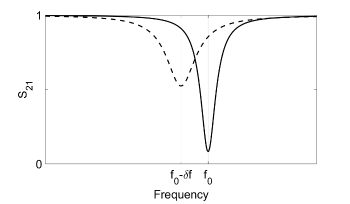
Figure 1. Spectral response of a resonator. The black line shows the transmission amplitude of a resonator in the dark with a resonance at frequency f0. The increase in quasiparticle density causes the resonance at f0 to move to a lower frequency, f0-δf, while simultaneously changing the amplitude of the signal (dashed line). Please click here to view a larger version of this figure.
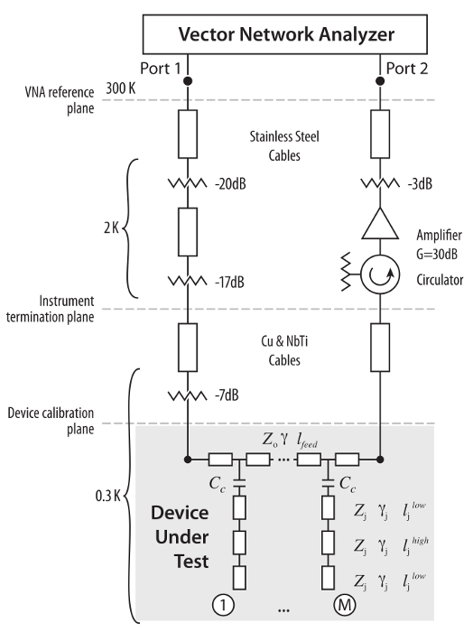
Figure 2. Schematic of the experimental set-up. The device under test consists of multiple Mo2N resonators coupled to a microwave Nb feedline through coupling capacitors, Cc. The stepped-impedance resonators are realized from low- and high-impedance microstrip transmission lines.11 It is designed to miniaturize the resonator and increase its harmonic resonance frequencies away from its fundamental resonant frequency. The transmission response through the feedline is measured with a VNA connected to the DUT via cables and other components. Modified from Cataldo et al.11 Please click here to view a larger version of this figure.
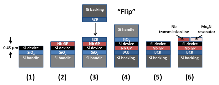
Figure 3. Microstrip resonator fabrication flow. This schematic illustrates the fabrication process summarized in Protocol 1. This process provides a means to fabricate superconducting circuitry on both sides of an ultra-thin single-crystal silicon dielectric layer. Modified from Patel et al.14 Please click here to view a larger version of this figure.
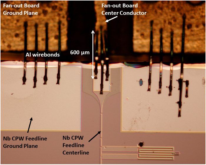
Figure 4. Micrograph of one end of the resonator chip mounted in the package. Al wire bond connections between the on-chip CPW Nb feedline and an off-chip fan-out board can be seen. Please click here to view a larger version of this figure.

Figure 5. Micrograph of Mo2N microstrip microwave resonator coupled to a Nb feedline for read-out. The H-shaped coupling region to the CPW feedline is located at the upper portion of the figure and is located on top of the oxide layer. The Y-shaped structure located in the bottom of the figure is used for coupling some of the resonators on other devices on the wafer to a microstrip transmission line. Further details about the resonator design can be found in Cataldo et al.11 and Patel et al.14 Please click here to view a larger version of this figure.
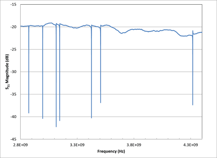
Figure 6. Measured transmission, S21, as a function of frequency (amplitude only) showing 7 Mo2N resonators coupled to a single microwave feedline. These data were taken in the cryogenic testbed at 0.3 K using a VNA. Please click here to view a larger version of this figure.
Discussion
The single-flip fabrication process provides a means for realizing superconducting resonators on both sides of a thin 0.45-µm single-crystal Si substrate. One may be motivated to use a single-crystal Si dielectric because it has more than an order of magnitude lower loss than deposited dielectrics (such as Si3N4) with loss tangents in the 4.0-6.5-GHz range < 1 x 10⁻⁵. 23-24 The ability to pattern features on both sides of this substrate allows one to employ a microstripline resonator design, which provides good immunity to stray light and low resonator-to-resonator crosstalk. The lift-off technique described allows the integrity of the Si surface to be maintained, because no roughening of its surface occurs during patterning of the superconducting Nb thin film.15 This fabrication process can be used for a variety of structures having a superconducting microstripline architecture, and anticipated future applications include using it for far-infrared spectrometers.25 Its main limitation is that the BCB used to glue the substrates together places an upper limit on the processing temperature (~250 °C).
Cryogenic measurements of the complex transmission of these resonator devices, as is described in the Protocol section, allow one to extract key materials parameters for superconducting and dielectric substrate materials and/or to monitor their response to far-infrared light. However, calibration and preparation of the test set-up is critical to the ability to do precise extractions of these material parameters. A standard SOLT calibration methodology was used to calibrate the transmission through the flexible SMA cables from the VNA to the input of the cryostat. The presence of the RF attenuator at the device input and the circulator at the device output are necessary to provide matched terminations. Post-measurement calibration can be carried out following the in-situ calibration procedure described in Cataldo et al.11 This in-situ calibration procedure moves the reference plane to the device input and output (labeled as the "device calibration plane" in Fig. 2). It should be noted that in Step 6 of Protocol section 4, an optimal spectral range and number of data points must be recorded, which provide both adequate sampling of the narrow resonator structures but also a span that goes beyond the resonators to enable the baseline to be removed correctly. Away from the resonators, the baseline becomes sufficiently decoupled to attain an unbiased amplitude calibration, thus reducing the error in parameters derived from the observed response.
To calibrate the VNA data in-situ, the following steps are performed: 1) Fit of the complex baseline through an analytical model physically motivated by the baseline response; 2) Normalization of the transmission's real and imaginary parts by forcing the transmission amplitude to be equal to one away from the resonators; 3) Correction for variations in gain and relocation of the reference plane at the DUT by dividing out the complex baseline fit.
The details of this calibration steps can be found in Sec. IV of Cataldo et al.11 After the data have been calibrated, the resonators can be modeled in one of two ways. In the first, a phenomenological model based on physically realizable rational functions enables extraction of the resonators' center frequencies and widths with an accuracy of 1% without explicitly specifying the circuit network (see Sec. V of Cataldo et al.11). In the second, an ABCD-matrix representation of the distributed transmission line circuit allows modeling of the observed response from the characteristic impedances, Z, and propagation constants, γ, with detailed knowledge of the device geometry (e.g., line lengths, l — see Fig. 2). Self-consistent constraints for the electromagnetic constitutive relations between the material's permittivity and permeability through Z and γ are enforced to extract parameters such as the resonators' kinetic inductance fraction and effective index with an accuracy of 2% when coupled with electromagnetic simulations (see Sec. VI of Cataldo et al.11). This allows studying the internal structure of the circuit.
Divulgations
The authors have nothing to disclose.
Acknowledgements
The authors acknowledge funding support from the National Aeronautics and Space Administration (NASA)'s ROSES and APRA programs. GC also acknowledges the Universities Space Research Association for administering his appointment at NASA.
Materials
| Microposit S-1811 Photoresist | Shipley | ||
| BCB | Dow | 3022-35 | |
| SOI wafers | SOITec | Fabricated with SmartCutTM process | |
| Mo | Kamis | 99.99% | |
| Nb | Kamis | 99.95% (excludes Ta) | |
| E-6 metal etch w/AES | Fujifilm | CPG Grade | |
| Acetone | JT Baker | 9005-05 | CMOS Grade |
| HF dip (1:10) | JT Baker | 5397-03 | |
| PMMA | Microchem | 950 PMMA A2 | |
| GE 7031 | General Electric | Low-temperature adhesive | |
| Cryogenic Microwave Amplifier | MITEQ | AF S3-02000400-08-CR-4 | 2-4 GHz, gain ~30dB |
| NbTi Semi-rigid SMA cables | Coax. Co. | SC-086/50-NbTi-NbTi | |
| Circulator | PamTech | CTD1229K | return loss > -20 dB from 2-4 GHz |
| RF attenuator | Weinschel | Model-4M | 7 dB attenuation |
| Flexible SMA cables | Teledyne-Storm | R94-240 | ACCU-TEST |
| Vector Network Analyzer | Agilent | N5242A PNA-X | |
| Liquid He-4 cryogen | Praxair | ||
| Liquid N2 cryogen | Praxair |
References
- Monfardini, A., et al. The Néel IRAM KID Arrays (NIKA). J. Low Temp. Phys. 167 (5-6), 834-839 (2012).
- Schlaerth, J. A., et al. The Status of Music: A Multicolor Sub/millimeter MKID Instrument. J. Low Temp. Phys. 167 (3-4), 347-353 (2012).
- Swenson, L. J., et al. MAKO: a pathfinder instrument for on-sky demonstration of low-cost 350 micron imaging arrays. Proc. SPIE. 8452, 84520P (2012).
- Mazin, B. A., Bumble, B., Meeker, S. R., O’Brien, K., McHugh, S., Langman, E. A superconducting focal plane array for ultraviolet, optical, and near-infrared astrophysics. Opt. Express. 20 (2), 1503-1511 (2012).
- Mazin, B. A. . Microwave Kinetic Inductance Detectors. , (2005).
- McHugh, S., et al. A readout for large arrays of Microwave Kinetic Inductance Detectors. Rev. Sci. Instrum. 83 (4), 044702 (2012).
- Mazin, B. A., et al. ARCONS: A 2024 Pixel Optical through Near-IR Cryogenic Imaging Spectrophotometer. Publ. Astron. Soc. Pac. 123 (933), 1348-1361 (2013).
- Zmuidzinas, J. Superconducting Microresonators: Physics and Applications. Annu. Rev. Condens. Matter Phys. 3, 169-214 (2012).
- Vijay, R., Slichter, D. H., Siddiqi, I. Observation of Quantum Jumps in a Superconducting. Artificial Atom. Phys. Rev. Lett. 106 (11), 110502 (2011).
- Krupka, J., Derzakowski, K., Tobar, M., Hartnett, J., Geyer, R. G. Complex permittivity of some ultralow loss dielectric crystals at cryogenic temperatures. Meas. Sci. Technology. 10 (5), 387-392 (1999).
- Cataldo, G., Wollack, E. J., Barrentine, E. M., Brown, A. D., Moseley, S. H., U-Yen, K. Analysis and calibration techniques for superconducting resonators. Rev. Sci. Instrum. 86 (1), 013103 (2015).
- Russell, D., Cleary, K., Reeves, R. Cryogenic probe station for on-wafer characterization of electrical devices. Rev. Sci. Instrum. 83 (4), 044703 (2012).
- Ranzani, L., Spietz, L., Popovic, Z., Aumentado, J. Two-port microwave calibration at millikelvin temperatures. Rev. Sci. Instrum. 84 (3), 034704 (2013).
- Patel, A., et al. Fabrication of MKIDS for the MicroSpec Spectrometer. IEEE Trans. Appl. Supercond. 23 (3), 2400404 (2013).
- Brown, A., Patel, A. High-Precision Thin Film Metal Liftoff Technique. , (2015).
- Laermer, F., Schlip, A. Method of anisotropically etching silicon. , (1996).
- Chen, D., Wang, Q., Shen, Z. A broadband microstrip-to-CPW transition. APMC 2005. Asian-Pac. Conf. Proc. 2 (4), (2005).
- Fano, U. Sullo spettro di assorbimento dei gas nobili presso il limite dello spettro d’arco. Il Nuovo Cimento. 12 (3), 154-161 (1935).
- Fano, U. Effects of Configuration Interaction on Intensities and Phase Shifts. Phys. Rev. 124 (6), 1866-1878 (1961).
- Marquezini, M. V., Kner, P., Bar-Ad, S., Tignon, J., Chemla, D. S. Density dependence of the spectral dielectric function across a Fano resonance. Phys. Rev. B. 57 (7), 3745-3748 (1998).
- Singh, R., Al-Naib, I., Cao, W., Rockstuhl, C., Koch, M., Zhang, W. The Fano Resonance in Symmetry Broken Terahertz Metamaterials. IEEE Trans. Terahertz Sci. Technol. 3 (6), 820-826 (2013).
- Giannini, V., Francescano, Y., Amrania, H., Phillips, C. C., Maier, S. A. Fano Resonances in Nanoscale Plasmonic Systems: A Parameter-Free Modeling Approach. Nano Lett. 11 (7), 2835-2840 (2011).
- O’Connell, A. D., et al. Microwave Dielectric Loss at Single Photon Energies and Millikelvin Temperatures. Appl. Phys. Lett. 92 (11), 112903 (2008).
- Weber, S. J., Murch, K. W., Slichter, D. H., Vijay, R., Siddiqi, I. Single Crystal Silicon Capacitor with Low Microwave Loss in the Single Photon Regime. Appl. Phys. Lett. 98 (17), 172510 (2011).
- Cataldo, G., Hsieh, W. T., Huang, W. C., Moseley, S. H., Stevenson, T. R., Wollack, E. J. Micro-Spec: an ultracompact, high-sensitivity spectrometer for far-infrared and submillimeter astronomy. Appl. Opt. 53 (6), 1094-1102 (2014).

