Growth of Gold Dendritic Nanoforests on Titanium Nitride-coated Silicon Substrates
Summary
This study presents a feasible procedure for synthesizing gold dendritic nanoforests on titanium nitride/silicon substrates. The thickness of gold dendritic nanoforests increases linearly within 15 min of a synthesis reaction.
Abstract
In this study, a high-power impulse magnetron sputtering system is used to coat a flat and firm titanium nitride (TiN) film on silicon (Si) wafers, and a fluoride-assisted galvanic replacement reaction (FAGRR) is employed for the rapid and easy deposition of gold dendritic nanoforests (Au DNFs) on the TiN/Si substrates. Scanning electron microscopy (SEM) images and energy-dispersive X-ray spectroscopy patterns of TiN/Si and Au DNFs/TiN/Si samples validate that the synthesis process is accurately controlled. Under the reaction conditions in this study, the thickness of the Au DNFs increases linearly to 5.10 ± 0.20 µm within 15 min of the reaction. Therefore, the employed synthesis procedure is a simple and rapid approach for preparing Au DNFs/TiN/Si composites.
Introduction
Gold nanoparticles have characteristic optical properties and localized surface plasmon resonances (LSPRs), depending on the size and shape of the nanoparticles1,2,3,4. Moreover, gold nanoparticles can significantly enhance plasmonic photocatalytic reactions5. Dendritic nanoforests stacked using gold nanoparticles have received considerable attention because of their noteworthy specific surface areas and robust LSPR enhancement6,7,8,9,10,11,12,13.
TiN is an extremely hard ceramic material and has remarkable thermal, chemical, and mechanical stability. TiN has distinctive optical properties and can be used for plasmonic applications with visible-to-near-infrared light14,15. Research has demonstrated that TiN can produce electromagnetic field enhancements, similar to Au nanostructures16. The deposition of copper17 or silver18,19,20 on TiN substrates for applications has been demonstrated. However, few studies have been performed on Au/TiN composite materials for applications. Shiao et al. have recently demonstrated potential applications of Au DNFs/TiN composites for photoelectrochemical cells21 and chemical degradation22.
Au can be synthesized on a TiN substrate by using a FAGRR23. The deposition condition of Au DNFs on TiN is crucial in the performance of applications. This study examines the growth of Au DNFs on a TiN-coated Si substrate.
Protocol
1. Sample preparation
- TiN substrate preparation using a high-power impulse magnetron sputtering system
- Cut a 4 inch n-type silicon wafer into 2 cm x 2 cm samples.
- Wash the samples using acetone, isopropanol, and deionized water.
- Dry them using an N2 spray for 5 min.
- Place the washed Si samples in a sample holder and place the sample holder into a high-power impulse magnetron sputtering (HiPIMS) chamber.
- Place a titanium target with a diameter of 4 inches on a sputtering cathode.
- Reduce the chamber pressure to less than 8 x 10⁻⁶ Torr by using a mechanical pump and cryopump.
- Use HiPIMS to deposit a Ti layer on a silicon wafer and deposit a TiN layer on the Ti layer. See Table 1 for the deposition parameters of Ti and TiN layers in HiPIMS.
- Au DNF preparation on TiN/Si substrates
- Place 24 mL of a reactant solution comprising 10 mM chloroauric acid (HAuCl4) and buffered oxide etchant solution comprising 11.4% NH4F and 2.3% HF into a Teflon container measuring 5 cm x 5 cm x 5 cm.
- Dip the substrates into the mixture solution for 3 min.
- Remove the sample and wash it using deionized water.
- Dry the sample using the N2 spray and then incubate it at 120 °C for 5 min to obtain Au DNFs/TiN/Si samples.
- Repeat the Au DNF preparation 10x.
2. Sample examination
- Scanning electron microscopy analyses
- Cut the sample into 0.4 cm x 0.8 cm with a tungsten pen, and clean it using the N2 spray.
- Coat a thin Pt film on the sample by an ion sputter coater for 50 s.
- Place the prepared sample into a scanning electron microscopy (SEM) instrument.
- Obtain SEM images by the scanning electron microscope and conduct element analysis21,22.
- X-ray diffraction analyses
- Place the sample into an X-ray diffraction (XRD) instrument.
- Obtain XRD patterns21,22.
Representative Results
Figure 1 depicts images of the Au DNFs/TiN/Si sample preparations. The silicon wafer was silvery white (Figure 1a). TiN/Si was golden yellow and had a homogeneous surface (Figure 1b), which indicated the uniform TiN coating on the silicon wafer. Au DNFs/TiN/Si was yellowish brown and less homogeneous on the surface (Figure 1c) because of the random distribution of Au DNFs.
Figure 2 presents the plan and cross-sectional SEM images of Au DNFs deposited on the TiN/Si substrates. The TiN layer had a uniform surface (Figure 2a), and the thickness of the TiN layer was approximately 300 nm (Figure 2b). At 1 min, small Au nuclei were observed everywhere (Figure 2c), some of which developed into a large nucleus similar to a sea urchin (Figure 2d). A single tree-like structure was formed at 3 min (Figure 2e,f), and these branching were observed to overlap at 5 min (Figure 2g,h). At 10 min, Au DNFs formed and covered the entire TiN layer (Figure 2i,j). At 15 min, dense Au DNFs were formed (Figure 2k), and the thickness of the DNFs reached 5 µm (Figure 2l).
Figure 3 shows the energy-dispersive X-ray spectroscopy (EDS) analysis results of TiN/Si and Au DNFs/TiN/Si. The indicated elements agreed with the synthesis procedure. Furthermore, the evident peaks could validate that the coating of TiN and the synthesis of Au DNFs were not polluted.
Figure 4 illustrates the variation of the thickness of the Au DNFs on the TiN/Si substrate with FAGRR time. The thickness of the Au DNFs increased linearly with synthesis time. The linear equation on the thickness and synthesis time, which ranged from 1 to 15 min, was expressed as follows: y = 0.296t + 0.649.
Figure 5 shows the XRD patterns of samples obtained by different deposition times. A strong (111) orientation of Au peaks was identified. The sharp cubic Au patterns, Au(111), Au(200), Au(220), and Au(311), agreed with JCPDS 04-0784. The increase in Au peaks with the deposition time corresponded to the growth of Au DNFs on the TiN/Si substrate. On the other hand, TiN peaks, namely TiN(111), TiN(200), TiN(220), and TiN(311), were evident at 1 min deposition, agreeing with JCPDS 38-1420. After 1 min, the signals of TiN gradually disappeared because the TiN/Si substrate was gradually covered by Au DNFs. These XRD results corresponded to previous reports21,22.
| Substrate | DC power (W) |
Impulse duration (µs) | Flow rate of Ar (sccm) | Flow rate of N2 (sccm) |
| Ti layer | 250 | 90 | 20 | – |
| TiN layer | 300 | 1000 | 30 | 1.5 |
Table 1: Conditions for preparing Ti and TiN. HiPIMS parameters for the deposition of Ti and TiN layers on a silicon wafer.
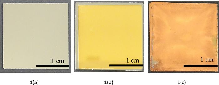
Figure 1: Sample appearance. Preparation of a 2 cm x 2 cm sample of (a) a silicon wafer, (b) TiN/Si, and (c) Au DNFs/TiN/Si. Please click here to view a larger version of this figure.
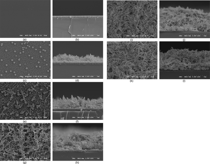
Figure 2: SEM pictures of samples. The SEM overhead and cross-section views of Au DNFs deposited on the TiN/Si substrates at (a and b) 0 min; (c and d) 1 min; (e and f) 3 min; (g and h) 5 min; (i and j) 10 min; (k and l) 15 min. Please click here to view a larger version of this figure.
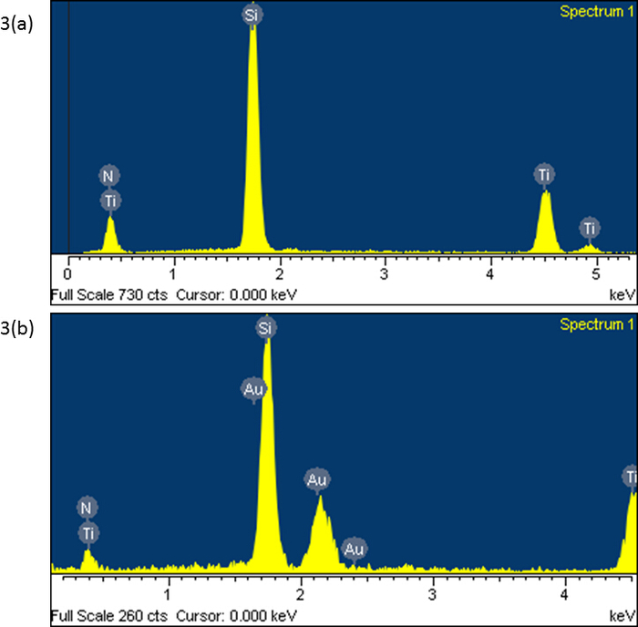
Figure 3: Elemental analysis. EDS spectrum of (a) TiN/Si and (b) Au DNFs/TiN/Si. Please click here to view a larger version of this figure.
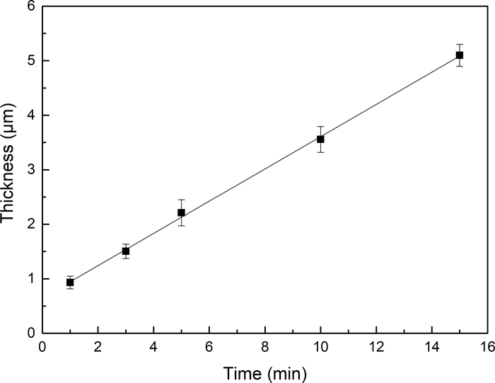
Figure 4: Au DNF thickness. The thickness of Au DNFs on TiN/Si substrate at various synthesis times (n = 10) Please click here to view a larger version of this figure.
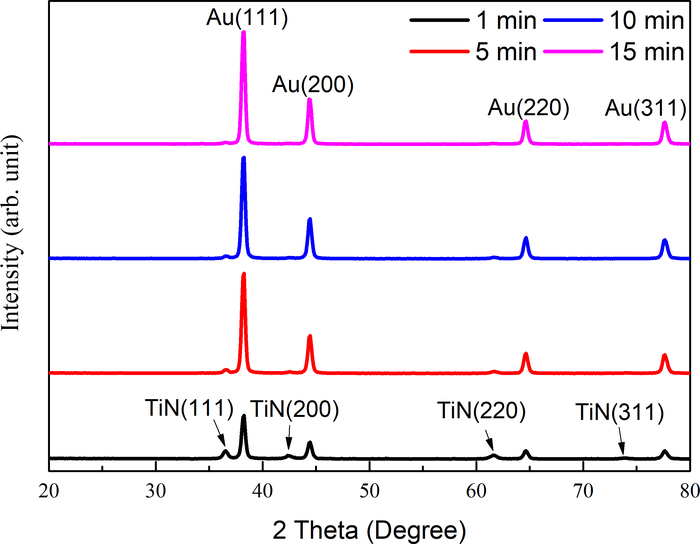
Figure 5: XRD patterns of samples. XRD patterns of Au DNFs on TiN/Si substrate at different synthesis times. Please click here to view a larger version of this figure.
Discussion
In this study, Au DNFs with multiple branch sizes were decorated on the surface of TiN/Si by using FAGRR. The deposition of the Au DNFs could be directly identified by a significant change in color. The thickness of the Au DNFs on TiN/Si increased to 5.10 ± 0.20 µm within 15 min, and this increase in thickness can be expressed using the following linear equation: y = 0.296t + 0.649, where the time varied from 1 to 15 min.
In FAGRR, the metal deposition is affected by the composition and the pH of the solution23. The deposition rate increases with the density of substrate surface defects. The thickness of the TiN layer decreases as the replacement reaction time increases. It is easy to remove Au DNFs from the TiN/Si substrates if the thickness of Au DNFs is thick enough.
Galvanic displacement reaction is more favorable for a metal with a higher redox potential23. In this study, the proposed facile and rapid electroless deposition process provides a feasible approach for preparing Au/TiN/Si composites which can be used as visible-light photocatalysts21,22. Using the same protocol, it is also possible to fabricate Au DNFs on other substrates, such as TiN/SiO2/Si, TiN/glass, TiN/ITO, and TiN/FTO, for applications in the future.
Divulgaciones
The authors have nothing to disclose.
Acknowledgements
This work was supported by the Ministry of Science and Technology, Taiwan, under contract numbers MOST 105-2221-E-492-003-MY2 and MOST 107-2622-E-239-002-CC3.
Materials
| Acetone | Dinhaw Enterprise Co. Ltd.,Taipei, Taiwan | ||
| Isopropanol | Echo Chemical Co. Ltd., Miaoli, Taiwan | TG-078-000000-75NL | |
| Buffered Oxide Etch | Uni-onward Corp., Hsinchu, Taiwan | UR-BOE-1EA | |
| Chloroauric Acid | Alfa Aesar., Heysham, United Kingdom | 36400.03 | |
| N-Type Silicon Wafer | Summit-Tech Company, Hsinchu, Taiwan | ||
| High-Power Impulse Magnetron Sputtering System (HiPIMS) | Melec GmbH, Germany | SPIK2000A | |
| Scanning Electron Microscope (SEM) | JEOL, Japan | JSM-7800F | |
| Ion Sputter Coater | Hitachi, Japan | E-1030 | |
| X-Ray Diffractometer (XRD) | PANalytical, The Netherlands | X'Pert PRO MRD |
Referencias
- Nehl, C. L., Hafner, J. H. Shape-dependent plasmon resonances of gold nanoparticles. Journal of Materials Chemistry. 18 (21), 2415-2419 (2008).
- Auguié, B., Barnes, W. L. Collective resonances in gold nanoparticle arrays. Physical Review Letters. 101 (14), 143902 (2008).
- Sakai, N., Fujiwara, Y., Arai, M., Yu, K., Tatsuma, T. Electrodeposition of gold nanoparticles on ITO: Control of morphology and plasmon resonance-based absorption and scattering. Journal of Electroanalytical Chemistry. 628 (1-2), 7-15 (2009).
- Shiao, M. H., Lai, C. P., Liao, B. H., Lin, Y. S. Effect of photoillumination on gold-nanoparticle-assisted chemical etching of silicon. Journal of Nanomaterials. 2018, 5479605 (2018).
- Ayati, A., et al. <a target="_blank" href="http://www.ncbi.nlm.nih.gov/entrez/query.fcgi?db=PubMed&cmd=Search&doptcmdl=Citation&defaultField=Title+Word&term=Photocatalytic+degradation+of+nitrobenzene+by+gold+nanoparticles+decorated+polyoxometalate+immobilized+TiO2+nanotubes.”>Photocatalytic degradation of nitrobenzene by gold nanoparticles decorated polyoxometalate immobilized TiO2 nanotubes. Separation and Purification Technology. 171, 62-68 (2016).
- Huang, T., Meng, F., Qi, L. Controlled synthesis of dendritic gold nanostructures assisted by supramolecular complexes of surfactant with cyclodextrin. Langmuir. 26 (10), 7582-7589 (2009).
- Lahiri, A., Wen, R., Kuimalee, S., Kobayashi, S. I., Park, H. One-step growth of needle and dendritic gold nanostructures on silicon for surface enhanced Raman scattering. CrystEngComm. 14 (4), 1241-1246 (2012).
- Lahiri, A., Wen, R., Kobayashi, S. I., Wang, P., Fang, Y. Unique and unusual pattern demonstrating the crystal growth through bubble formation. Crystal Growth & Design. 12 (3), 1666-1670 (2012).
- Lahiri, A., et al. Photo-assisted control of gold and silver nanostructures on silicon and its SERRS effect. Journal of Physics D: Applied Physics. 46 (27), 275303 (2013).
- Lv, Z. Y., et al. Facile and controlled electrochemical route to three-dimensional hierarchical dendritic gold nanostructures. Electrochimica Acta. 109, 136-144 (2013).
- Dutta, S., et al. Mesoporous gold and palladium nanoleaves from liquid–liquid interface: enhanced catalytic activity of the palladium analogue toward hydrazine-assisted room-temperature 4-nitrophenol reduction. ACS Applied Materials & Interfaces. 6 (12), 9134-9143 (2014).
- Lin, C. T., et al. Rapid fabrication of three-dimensional gold dendritic nanoforests for visible light-enhanced methanol oxidation. Electrochimica Acta. 192, 15-21 (2016).
- Lahiri, A., Kobayashi, S. I. Electroless deposition of gold on silicon and its potential applications. Surface Engineering. 32 (5), 321-337 (2016).
- White, N., et al. Surface/interface analysis and optical properties of RF sputter-deposited nanocrystalline titanium nitride thin films. Applied Surface Science. 292, 74-85 (2014).
- Zhao, J., et al. Surface enhanced Raman scattering substrates based on titanium nitride nanorods. Optical Materials. 47, 219-224 (2015).
- Lorite, I., Serrano, A., Schwartzberg, A., Bueno, J., Costa-Krämer, J. L. Surface enhanced Raman spectroscopy by titanium nitride non-continuous thin films. Thin Solid Films. 531, 144-146 (2013).
- O’Kelly, J. P., et al. Room temperature electroless plating copper seed layer process for damascene interlevel metal structures. Microelectronic Engineering. 50 (1), 473-479 (2000).
- Cesiulis, H., Ziomek-Moroz, M. Electrocrystallization and electrodeposition of silver on titanium nitride. Journal of Applied Electrochemistry. 30 (11), 1261-1268 (2000).
- Wu, Y., Chen, W. C., Fong, H. P., Wan, C. C., Wang, Y. Y. Displacement reactions between metal ions and nitride barrier layer/silicon substrate. Journal of the Electrochemical Society. 149 (5), G309-G317 (2002).
- Koo, H. C., Ahn, E. J., Kim, J. J. Direct-electroplating of Ag on pretreated TiN surfaces. Journal of the Electrochemical Society. 155 (1), D10-D13 (2008).
- Shiao, M. H., et al. Novel gold dendritic nanoflowers deposited on titanium nitride for photoelectrochemical cells. Journal of Solid State Electrochemistry. 22 (10), 3077-3084 (2018).
- Shiao, M. H., Lin, C. T., Zeng, J. J., Lin, Y. S. Novel gold dendritic nanoforests combined with titanium nitride for visible-light-enhanced chemical degradation. Nanomaterials. 8 (5), 282 (2018).
- Carraro, C., Maboudian, R., Magagnin, L. Metallization and nanostructuring of semiconductor surfaces by galvanic displacement processes. Surface Science Reports. 62 (12), 499-525 (2007).

