Preparation of ZnO Nanorod/Graphene/ZnO Nanorod Epitaxial Double Heterostructure for Piezoelectrical Nanogenerator by Using Preheating Hydrothermal
Summary
One-step fabrication method for obtaining freestanding epitaxial double heterostructure is presented. This approach could achieve ZnO coverage with a higher number density than that of the epitaxial single heterostructure, leading to a piezoelectric nanogenerator with an increased output electrical performance.
Abstract
Well-aligned ZnO nanostructures have been intensively studied over the last decade for remarkable physical properties and enormous applications. Here, we describe a one-step fabrication technique to synthesis freestanding ZnO nanorod/graphene/ZnO nanorod double heterostructure. The preparation of the double heterostructure is performed by using thermal chemical vapor deposition (CVD) and preheating hydrothermal technique. In addition, the morphological properties were characterized by using the scanning electron microscopy (SEM). The utility of freestanding double heterostructure is demonstrated by fabricating the piezoelectric nanogenerator. The electrical output is improved up to 200% compared to that of a single heterostructure owing to the coupling effect of the piezoelectricity between the arrays of ZnO nanorods on the top and bottom of graphene. This unique double heterostructure have a tremendous potential for applications of electrical and optoelectrical devices where the high number density and specific surface area of nanorod are needed, such as pressure sensor, immuno-biosensor and dye-sensitized solar cells.
Introduction
Recently, the portable and wearable electronics devices became an essential element for a comfortable life owing to the nanotechnology development, which results in the tremendous demands for a power source in the range of microwatt to milliwatt. Considerable approaches for the power source of portable and wearable devices have been achieved by the renewable energy, including solar energy 1,2, thermal 3,4 and mechanical source 5,6. Piezoelectric nanogenerator have been intensively studied as one of possible candidate for energy harvesting device from environments, such as rustling the leaf 7, sound wave 8 and movement of human being 9. The primary principle underlying the nanogenerator is the coupling between the piezoelectric potential and dielectric material as a barrier. The piezoelectric potential generated in strained material induces the transient current that flows through the external circuit, which balances the potential at the interface between piezoelectric and dielectric material. The performance of nanogenerator would be improved by using nanostructure of piezoelectric material due to robustness under robustness under high stress and responsiveness to tiny deformation 10.
One-dimensional zinc oxide nanostructure is a promising component for piezoelectric materials in nanogenerator due to its attractive properties, e.g., its high piezoelectricity (26.7 pm/V) 11, optical transparency 12, and facile synthesis by using chemical process 13. Hydrothermal approach for growing the well aligned ZnO nanorod receives a great attention due to low cost, environmental friendly synthesis and potential for easy scaling up. Moreover, the preheating hydrothermal technique is easily controllable in experimental condition, resulting in many kinds of novel nanostructures, such as nanoleaves 14, nanoflowers 15 and nanotubes 16. The novel nanostructures enable a beneficial effect on performance of the electric and optoelectric devices wherever the high specific surface area of material is demanded.
In this protocol, we describe the experimental procedures for synthesis of more novel nanostructure (i.e., freestanding double heterostructure). The growth of ZnO nanorod at interface between graphene and polyethylene terephthalate (PET) substrate leads to the self-elevating the ZnO nanorod/graphene single heterostructure, yielding the freestanding double heterostructure. Furthermore, the feasible application of this unique nanostructure for electronic and optoelectric devices is demonstrated by fabricating a piezoelectric nanogenerator. Freestanding double heterostructure provides not only a high specific surface area but also a high number density of nanorod in a given area. This unique nanostructure has a tremendous potential for applications of electrical and optoelectrical devices, such as pressure sensor, immuno-biosensor and dye-sensitized solar cells.
Protocol
1. Chemical Vapor Deposition (CVD) Growth of Single Layered Graphene
Note: The graphene used in this study was grown on copper (Cu) foil using the thermal chemical vapor deposition (CVD) technique (Figure 1A). Growth is uniform over an area of 2 cm x 10 cm for this system.
- Wash the Cu foil (2 cm x 10 cm) with mild flow of acetone, isopropyl alcohol (IPA) and distilled water, respectively.
- Place the cleaned Cu foil in a 2 in. quartz tube (Figure 1B), and then purge the chamber with vacuum (approximately 1 mTorr) for 10 min by using rotary pump.
- Configure the temperature of digitalized furnace and ramp up the furnace to 995 °C, while maintaining the desired flow rates (100 sccm for Argon and 50 sccm for hydrogen) (Figure 1C).
- Introduce the 20 sccm of methane (CH4) for 10 min to grow the single layered graphene. Maintain the 80 sccm of Argon and 20 sccm of hydrogen throughput the process.
- Allow the furnace to cool down to RT within 5 min with the flow rates specified in the step 1.4. Purge the chamber again with Argon at 100 sccm.
2. Preparation of Graphene/Polyethylene Terephthalate (PET) Substrate
- Place the graphene grown Cu foil (1.5 cm x 2 cm) on the glass slide, and fix the edges by commercial tape (Figure 2A).
- Spin coat a layer of poly(methyl methacrylate) (PMMA) at 500 rpm for 5 sec and then 3,000 rpm for 30 sec (Figure2B). Then, bake the PMMA-coated Cu foil substrate at 60 °C for 2 min to remove solvent residue.
- Dice the PMMA coated Cu foil into smaller piece 1 cm x 1.5 using razor blade.
- Immerse PMMA coated Cu foil into Ni etchant reservoir (more than 500 ml) by placing the Cu foil face down for 30 min. This leaves the floating PMMA/graphene layer on etchant solution (Figure 2C). A piece of PMMA-coated Cu foil is enough for the experiment forward.
- Scoop PMMA/graphene layer up on slide glass, and then immerse PMMA/graphene layer into DI water reservoir. Repeat twice. Finally, scoop PMMA/graphene layer up on PET substrate (Figure 2D), and then bake the substrate at 105 °C for 2 min to remove water residue.
- Remove the PMMA layer by dipping in warm acetone (60 °C) for 10 min.
3. Synthesis of ZnO Nanorod/Graphene/ZnO Nanorod Epitaxial Double Heterostructure
- Begin with heating the precursor solution with 40 mM zinc nitrate hexahydrate, 40 mM hexamethylenetetramine (HMT) and 9 mM polyethylenimine (PEI) in DI water for 60 min at 95 °C in convection oven (Figure 3A). Namely, preheating process.
- While preheating process, fully cover the solution with 5 mM zinc acetate in ethanol on the substrate and spin coat a layer of zinc acetate on the graphene/PET substrate at 500 rpm for 5 sec and then 2,000 rpm for 60 sec (Figure 3B and Figure 3C).Then, bake the substrate at 200 °C for 30 min. Repeat twice. The thickness of layer is approximately 30 nm.
- Immerse the seed-coated graphene/PET substrate into preheated solution by placing the substrate face down at 95 °C (Figure 3D). Determine the heating time for the desired nanostructure; i.e., single heterostructure (t < 12 hr, Figure 3E) and double heterostructure (t > 12 hr, Figure 3F).
- Carefully spray ethanol on the substrate and dry it at RT for 1 hr.
Note : For scanning electron microscopy (SEM), dice the sample into smaller piece 5 mm x 5 mm using razor blade and mount the sample on SEM stage.
4. Fabrication of Piezoelectric Nanogenerator
Note: Piezoelectric nanogenerator in this study has the three electrodes (top, middle, bottom). Use the indium tin oxide (ITO) coated PET as the bottom electrode (Figure 4A).
- Spin coat a layer of polydimethylsiloxane (PDMS) at 500 rpm for 5 sec and then 6,000 rpm for 60 sec to form the insulating layer between ITO and ZnO nanorod (Figure 4B). The thickness of layer is approximately 3 µm.
- Fully cure the substrate at 80 °C for 2 hr in convection oven.
- Transfer the graphene to PDMS coated ITO/PET substrate by using the method in Section 2 (Figure 4C).
- Synthesize the double heterostructure on the substrate by using the method in Section 3 (Figure 4D).
- Spin coat a layer of PDMS at 500 rpm for 5 sec and then 5,000 rpm for 60 sec to improve the robustness and durability of the ZnO nanorod, and then fully cure it at 80 °C for 2 hr (Figure 4E). The thickness of layer is approximately 8 µm.
- Cover the substrate with ITO-coated PET as the top electrode (Figure 4F).
5. Electrical Performance Measurement Setup
Note: We set up custom-made equipment for electrical performance characterization using linear motor, commercial scale and oscilloscope. Build the frame for vertically supporting the linear motor and place the commercial scale under the linear motor as shown in Figure 5A. The scale should be sensitive to small weight (0.02 kg – 20 kg).
- Place the nanogenerator on a scale, and then connect the electrodes of nanogenerator to sensing probes of oscilloscope (Figure 5A and 5B).
- Set up the initial and final positions and speed of linear motor while carefully monitoring the weight in the scale.
Tip : Configure the initial position where nanogenerator is slightly contacted with measurement setup. Speed of linear motor determines the strain rate. - Start the linear motor and monitor the voltage signal with time. Save the time-dependent voltage signal in flash memory. Strain rate: 100 mm/sec and applied load: 50 N.
Representative Results
The scanning electron microscopy (SEM) images shown in Figure 6 present the morphologies of hydrothermally grown ZnO nanorods. The preheating hydrothermal technique can result in two different nanostructures depending on the growth time. Figure 6A shows a typical image of ZnO nanorod on graphene/PET substrate at the growth time of 5 hr. In contrast, the image shown in Figure 6B indicates that the growth of ZnO nanorod at the growth time of 12 hr is successfully proceeded not only on the top of graphene but also on the bottom of graphene. Both ZnO nanorods are vertically aligned to the graphene layer, with average lengths of 2.49 and 0.70 µm, respectively. In addition, the length of ZnO nanorod on the bottom of graphene is increased approximately 2 times as the growth time increases up to 24 hr, as shown in Figure 6C. The growth of ZnO nanorod on the bottom of graphene is carried out over a large scale (>30 µm) and results in the self-elevation of ZnO nanorod/graphene construct, thereby forming freestanding double heterostructure (Figure 6D).
Figure 7A shows a photograph of the piezoelectric nanogenerator, which composed of the freestanding double heterostructure and two ITO-coated PET substrates as the top and bottom electrode. The electrical output is originated from the nanogenerator rather than measurement system, which is confirmed by polarity-switching measurement (Figure 7B and 7C). The output voltages from the arrays of ZnO nanorod on the top and bottom of graphene are observed up to 0.5 V and 0.3 V, respectively, by applying the periodic compress-release loads of 49 N (Figure 7E and 7F). Furthermore, the both arrays of ZnO nanorod produce the enhanced output voltage and current with average values of 0.9 V and 70 nA, respectively. The simulation result performed by COMSOL package reveals that the polarity of ZnO nanorod on the top and bottom graphene are reverse and good agreement between the results obtained from experiments and simulation (Figure 7D).
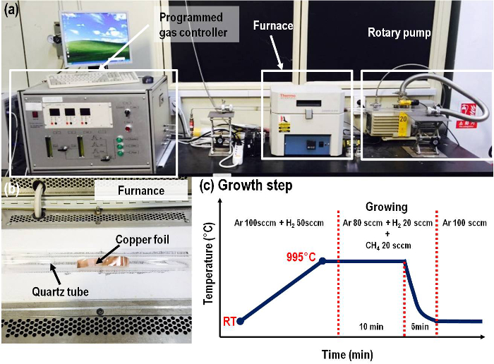
Figure 1. Growth of single layer graphene. (A) An image of experimental setup for thermal CVD. (B) Cu foil placement in growth furnace and (C) Growth step for single layer graphene. Please click here for a larger version of this figure.

Figure 2. Process flow of graphene transfer by using fishing method. Please click here for a larger version of this figure.
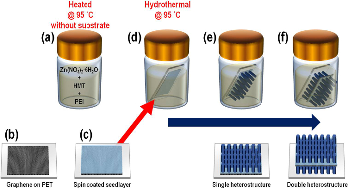
Figure 3. Synthesis process for the freestanding double heterostructure. Please click here for a larger version of this figure.

Figure 4. Schematic of the fabrication process for piezoelectric nanogenerator. Please click here for a larger version of this figure.
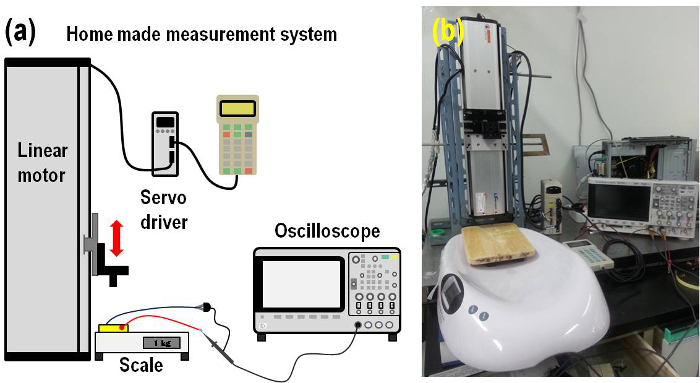
Figure 5. Electrical measurement setup. (A) Home-made measurement system schematic and (B) An photograph of measurement system. Please click here for a larger version of this figure.
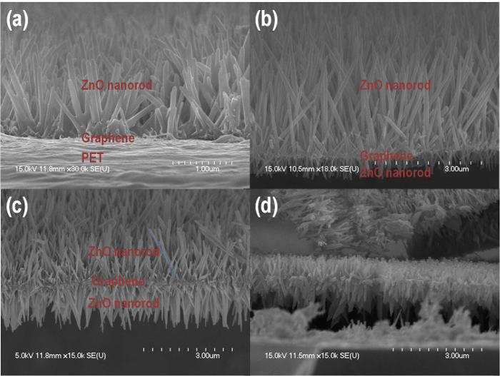
Figure 6. SEM images of hydrothermally grown ZnO nanorod. (A) Single heterostructure after 5 hr of growth. Double heterostructure after 12 hr (B) and 24 hr (C) of growth and (D) Freestanding double heterostructure. Please click here for a larger version of this figure.
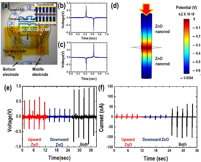
Figure 7. Representative results for piezoelectric nanogenerator. (A) An photograph of fabricated nanogenerator. Output voltages in forward (B) and reverse (C) connections. (D) COMSOL simulation of piezoelectric potential along a ZnO nanorod under axial strain. The dimensions of the nanorod are L = 600 nm and a = 60 nm and external force is 80 nN. Output voltages (E) and currents (F) of nanogenerator. Please click here for a larger version of this figure.
Discussion
Please note that the high quality (>99.8%, annealed) of Cu foil should be considered as a substrate for successful growth of single layer graphene. Otherwise, the single layer graphene is not uniformly grown over the Cu foil, leading to dramatically decrease in conductivity of graphene. A 1 hr annealing at high temperature would help the improvement of the Cu foil crystallinity as well as removal of any contaminants from the Cu foil.
The growth of ZnO nanorod depends on the conditions for preheating hydrothermal, hence, the optimal concentration, temperature and time for growth have to carefully be calibrated. The concentration of zinc nitrate hexahydrate and HMT determines the diameter of ZnO nanorod, the additive PEI would not only provide the enhancement in aspect ratio of ZnO nanorod but also help continuous ZnO growth for long time 17,18.
The SEM images of typical freestanding single and double heterostructure are shown in Figure 6. As can be seen from these figures, the array of ZnO nanorods on the bottom of graphene begins to grow after 12 hr of growth, and their length linearly increase from 0.71 to 1.56 µm. Furthermore, the length of ZnO nanorods on the top of graphene is linearly increase before 12 hr, and then saturated approximately 2 µm after the growth of downward-grown ZnO nanorod. This result indicates that the ZnO nanorod growth obeys the manner of routine hydrothermal before 12 hr, but the double heterostructure begin to grow after 12 hr due to decomposed seed layer and the vacancy defect of graphene 19. Since we just regulated the growth time of typical hydrothermal technique to fabricate double heterostructure, the methodology proposed here can be used for other hydrothermally grown metal oxides, such as TiO2, SnO2 and Fe3O4.
For electrical measurements, it is necessary to examine whether or not the electric signal come from the fabricated nanogenerator. Triboelectricity between nanogenerator and measurement setup leads to electrical noise, and interrupts the accurate observation of piezoelectric performance. This is avoided by carefully configuring the initial position where nanogenerator is slightly contacted with measurement setup.
In summary, this manuscript details the facile protocols for fabricating a ZnO nanorod/graphene/ZnO nanorod epitaxial double heterostructure. The versatile approach to construct double heterostructure could enhance not only the number density of ZnO nanorod but also the specific surface area of double heterostructure in a given region. This approach thus utilizes two consecutive growth techniques to precisely construct unique nanomaterials into spatially arranged structures that can serve as functional materials for the number of electronic and optoelectronic applications such as touchpad electronics, smart gloves, implantable devices, and biosensors.
Divulgazioni
The authors have nothing to disclose.
Acknowledgements
This work was supported by the National Research Foundation of Korea (NRF) grant funded by the Korea government (MSIP) (No.2014R1A2A1A11051146). This work was also supported by National Research Foundation of Korea Grant funded by the Korean Government (NRF-2014R1A1A2058350).
Materials
| Cu foil | Alfa Aesar | 13382 | |
| poly(methyl methacrylate) (PMMA) | Aldrich | 182230 | |
| zinc nitrate hexahydrate | Sigma-Aldrich | 228732 | |
| hexamethylenetetramine (HMT) | Sigma-Aldrich | 398160 | |
| polyethylenimine (PEI) | Sigma-Aldrich | 408719 | |
| indium tin oxide (ITO) coated PET | Aldrich | 639303 | |
| Silicone Elastomer Kit | Dow Corning | Sylgard 184 a, b | |
| Nickel Etchant Type1 | Transene Company | 41212 |
Riferimenti
- Lee, S., Lee, Y., Park, J., Choi, D. Stitchable organic photovoltaic cells with textile electrodes. Nano Energy. 9, 88-93 (2014).
- Pan, S., et al. Wearable solar cells by stacking textile electrodes. Angew. Chem.-Int. Edit. 53, 6110-6114 (2014).
- Yang, Y., et al. Pyroelectric nanogenerators for harvesting thermoelectric energy. Nano Lett. 12, 2833-2838 (2012).
- Lee, J. H., et al. Highly stretchable piezoelectric-pyroelectric hybrid nanogenerator. Adv. Mater. 26, 765-769 (2014).
- Zhong, J., et al. Finger typing driven triboelectric nanogenerator and its use for instantaneously lighting up LEDs. Nano Energy. 2, 491-497 (2013).
- Tang, W., Han, C. B., Zhang, C., Wang, Z. L. Cover-sheet-based nanogenerator for charging mobile electronics using low-frequency body motion/vibration. Nano Energy. 9, 121-127 (2014).
- Li, S., Yuan, J., Lipson, H. Ambient wind energy harvesting using cross-flow fluttering. J. Appl. Phys. 109, 026104 (2011).
- Cha, S. N., et al. Sound-driven piezoelectric nanowire-based nanogenerators. Adv. Mater. 22, 4726-4730 (2010).
- Bai, P., et al. Integrated multilayered triboelectric nanogenerator for harvesting biomechanical energy from human motions. ACS Nano. 7, 3713-3719 (2013).
- Xu, S., Wang, Z. L. One-dimensional ZnO nanostructures: Solution growth and functional properties. Nano Res. 4, 1013-1098 (2011).
- Zhao, M. -. H., Wang, Z. -. L., Mao, S. X. Piezoelectric characterization of individual zinc oxide nanobelt probed by piezoresponse force microscope. Nano Lett. 4, 587-590 (2004).
- Nam, G. -. H., Baek, S. -. H., Cho, C. -. H., Park, I. -. K. A flexible and transparent graphene/ZnO nanorod hybrid structure fabricated by exfoliating a graphite substrate. Nanoscale. 6, 11653-11658 (2014).
- Zou, X., Fan, H., Tian, Y., Yan, S. Facile hydrothermal synthesis of large scale ZnO nanorod arrays and their growth mechanism. Mater. Lett. 107, 269-272 (2013).
- Qiu, J., et al. Single-crystalline twinned ZnO nanoleaf structure via a facile hydrothermal process. J. Nanosci. Nanotechnol. 11, 2175-2184 (2011).
- Qiu, J., et al. Synthesis and characterization of flower-like bundles of ZnO nanosheets by a surfactant-free hydrothermal process. J. Nanomater. 2014, 281461 (2014).
- Sun, Y., Riley, D. J., Ashfold, M. N. R. Mechanism of ZnO nanotube growth by hydrothermal methods on ZnO Film-coated Si substrates. J. Phys. Chem. B. 110, 15186-15192 (2006).
- Qiu, J., et al. The growth mechanism and optical properties of ultralong ZnO nanorod arrays with a high aspect ratio by a preheating hydrothermal method. Nanotechnology. 20, 155603 (2009).
- Qiu, J., et al. Solution-derived 40 µm vertically aligned ZnO nanowire arrays as photoelectrodes in dye-sensitized solar cells. Nanotechnology. 21, 195602 (2010).
- Shin, D. -. M., et al. Freestanding ZnO nanorod/graphene/ZnO nanorod epitaxial double heterostructure for improved piezoelectric nanogenerators. Nano Energy. 12, 268-277 (2015).

