Elaborate Control of Inkjet Printer for Fabrication of Chip-based Supercapacitors
Summary
This paper provides a technique for manufacturing chip-based supercapacitors using an inkjet printer. Methodologies are described in detail to synthesize inks, adjust software parameters, and analyze the electrochemical results of the manufactured supercapacitor.
Abstract
There are tremendous efforts in various fields to apply the inkjet printing method for the fabrication of wearable devices, displays, and energy storage devices. To get high-quality products, however, sophisticated operation skills are required depending on the physical properties of the ink materials. In this regard, optimizing the inkjet printing parameters is as important as developing the physical properties of the ink materials. In this study, optimization of the inkjet printing software parameters is presented for fabricating a supercapacitor. Supercapacitors are attractive energy storage systems because of their high power density, long lifespan, and various applications as power sources. Supercapacitors can be used in the Internet of Things (IoT), smartphones, wearable devices, electrical vehicles (EVs), large energy storage systems, etc. The wide range of applications demands a new method that can fabricate devices in various scales. The inkjet printing method can break through the conventional fixed-size fabrication method.
Introduction
In the past decades, multiple printing methods have been developed for various applications, including wearable devices1, pharmaceuticals2, and aerospace components3. The printing can be easily adapted for various devices by simply changing the materials to be used. Moreover, it prevents the wastage of raw materials. To manufacture electronic devices, several printing methods such as screen printing4, push-coating5, and lithography6 have been developed. Compared to these printing technologies, the inkjet printing method has multiple advantages, including reduced material waste, compatibility with multiple substrates7, low cost8, flexibility9, low-temperature processing10, and ease of mass production11. However, the application of the inkjet printing method has hardly been suggested for certain sophisticated devices. Here, we present a protocol establishing detailed guidelines to use the inkjet printing method for printing a supercapacitor device.
Supercapacitors, including pseudocapacitors and electrochemical double-layer capacitors (EDLCs), are emerging as energy storage devices that can complement conventional lithium-ion batteries12,13. Especially, EDLC is a promising energy storage device because of its low cost, high power density, and long cycle life14. Activated carbon (AC), having high specific surface area and conductivity, is used as electrode material in commercial EDLCs15. These properties of AC allow EDLCs to have a high electrochemical capacitance16. EDLCs have the passive volume in devices when the conventional fixed-size fabrication method is used. With inkjet printing, the EDLCs can be fully integrated into the product design. Therefore, the device fabricated using the inkjet printing method is functionally better than that fabricated by existing fixed-size methodologies17. The fabrication of EDLCs using the efficient inkjet printing method maximizes the stability and longevity of EDLCs and provides a free-form factor18. The printing patterns were designed by using a PCB CAD program and converted to Gerber files. The designed patterns were printed using an inkjet printer because it has precise software-enabled control, high material throughput, and printing stability.
Protocol
1. Design of pattern using PCB CAD program
- Run the CAD program. Click on the File button atop the program window. To form a new project file, click on the Nouveau and Project buttons.
- To generate the board file, click on the File, Nouveau, and Board buttons in order. Set the grid size, multiple, and alt values by clicking on the mesh-shaped Grid button at the top left of the created Board File window (or clicking on View and Grid in order at the top of the window).
- Change both the grid size and alt value from mm to inch so that the inkjet printer can read the PCB CAD pattern. Press Finest to make fine adjustments.
- Design the pattern of the current collector and EDLC line in an interdigitated form. Design the gel polymer electrolyte (GPE) pattern and current collector pads in a rectangular form (Figure 1).
NOTE: Pattern width: 43 mm, pattern height: 55 mm, line length: 40 mm, line width: 1.0 mm, line-to-line space: 1.5 mm, and pad size: 15 x 5 mm2.- Since the final pattern consists of three types (conductive line, EDLC, and GPE), set the three layers as follows.
- Click on View and Layer Settings in order at the top of the window. Create new layers by clicking on the New Layer button at the bottom left of the Visible Layers window.
- In the new window (New Layer), set up the name and color for the new layer. For visually distinguishing the layers, set the names of the three layers to Current Collector, EDLC, and GPE, and change the corresponding colors by clicking on the box to the right of Color.
- Press Line at the bottom left of the screen, click on the main field (black background), and drag to draw a line. To change the thickness of the line, input the value of Width located at the top center in inch scale (1.0 mm = 0.0393701 inch).
- To edit the length of a line, right-click on the line and click on Properties at the bottom. In the From and To fields, input the x and y values of the starting and ending points.
- To set the reference point of the pattern, set the upper-left corner of the pattern shown in Figure 1 to (0,0). Draw the rest of the pattern based on the above information.
- To set the drawn pattern to the desired layer, right-click on the pattern and click on Properties. Then, click on Layer, and choose the desired layer.
- To draw rectangular patterns of the current collector pad and GPE, press Rect at the bottom left of the main window. Click and drag on the screen (main field) where the previously drawn pattern exists.
- To edit, right-click on the rectangular surface and click on Properties at the bottom. Input the upper left (x,y) value and the lower right (x,y) value of the rectangle in the From and To fields, respectively. Set the rectangle to the desired layer as mentioned in step 1.4.5.
- Since the final pattern consists of three types (conductive line, EDLC, and GPE), set the three layers as follows.
- Convert the CAD file of the designed pattern into the Gerber file format that is read by the inkjet printer.
- Before converting the designed pattern file, save the Board File in .brd format. To save, click on File, and then on Save (or press ctrl + S on the keyboard).
- After saving, click on File at the top of the window and click on CAM Processor. To create a Gerber file of the desired layer, modify the items under Gerber of Output Files on the left side of the window, as follows.
- First, delete the sub-lists such as Top Copper and Bottom Copper by pressing the '-' below. Press '+' and click on New Gerber Output to create Gerber output.
- On the right side of the screen, set the layer name in Name and Function à Copper by pressing the gear on the right. Set Layer Type à Top and set Gerber Layer Number of the current collector, EDLC and GPE to L1, L2, L3, respectively.
- In the Layers window at the bottom of Gerber File, click on Edit Layers at the bottom left, and select each desired layer.
- To set the name of the output file to be created, set the Gerber Filename of Output at the bottom of the window to %PREFIX/%NAME.gbr.
- Finally, click on Save Job at the top left of the window to save the settings. Click on Process Job at the bottom right to create a Gerber file.
2. Ink synthesis
NOTE: Flexible Ag ink is used as conductive ink for the current collector line and pads.
- Prepare EDLC ink using terpineol, ethylcellulose, activated carbon (AC), Super-P, polyvinylidene difluoride (PVDF), and Triton-X as follows.
- Use 2,951 µL of terpineol with high viscosity as the solvent and 1.56 g of ethyl cellulose as a thickener. Set the ratio of AC to Super-P to PVDF as 7:2:1 with a total weight of 1.8478 g. In addition, use 49 µL of Triton-X as a surfactant for mixing.
- Mix all the materials for 30 min using a planetary mixer. Place the well-mixed electrode material in a cartridge for the inkjet printer and centrifuge it at 115 x g for 5 min.
- Prepare GPE ink using propylene carbonate (PC), PVDF, and lithium perchlorate (LiClO4) as follows.
- Use PC as the solvent, PVDF as the polymer matrix, and LiClO4 as the salt. Weigh all components of GPE such that the final molar concentration of LiClO4 is 1 M, and the final weight % of PVDF is 5 wt%.
- Stir all the components at 140 °C for 1 h until dissolution. After stirring, cool the GPE ink sufficiently and place it into the ink cartridge.
3. Inkjet printer software parameter set-up
- Run the printer program. Click on the Print button, select Simple, and then select Flexible Conductive Ink in order as shown in Figure 2.
- Upload the Gerber file of the designed pattern by following the 1 arrow in Figure 3. Choose and open the Gerber file of the conductive line (see 2 and 3 arrows in Figure 3). Click on the NEXT button as indicated by the 4 arrow.
- Fix the PCB board as shown in Figure 4A, and mount the probe as shown in Figure 4B.
- Adjust the zero point of the PCB printer through the probe by clicking on the OUTLINE button (see the 1,4 red arrow in Figure 5).
NOTE: The probe moves over the PCB board while showing the outline of the pattern (see the bottom right of Figure 5). - Move the pattern image on the screen by dragging (see the yellow dashed arrow in Figure 5). Click on the OUTLINE button once more to check whether the probe moves through the desired path. Click on NEXT (indicated by the 5 arrow in Figure 5).
- Click on PROBE to measure the height of the substrate for checking whether the substrate is flat (Figure 6).
NOTE: The probing region on the substrate is automatically selected by the program built into the printer. - Remove the probe once the height measurement is completed. Insert the ink cartridge into the ink dispenser and connect the nozzle (inner diameter: 230 µm) to prepare the dispenser.
- Mount each ink (conductive line, EDLC, GPE) dispenser, and print a sample pattern by pressing the CALIBRATE button, while adjusting the parameters of each ink (Figure 7).
- Visually check the printing result and record the parameter values for each ink. See Representative Results for details.
4. Printing the conductive line
NOTE: Since steps 4.1. to 4.7. overlap with section 3, they are only briefly summarized below.
- Run the inkjet printer program and click on Print in the start menu and select Simple (Figure 1).
- Click on the Choose File button next to Ink to load the designed pattern file and click on NEXT (Figure 3).
- Fix the PCB board onto the printer and install the probe (Figure 4).
- Check the position of the pattern on the substrate and measure the height of the substrate (Figure 5 and Figure 6).
- Remove the probe, and then mount the conductive ink (flexible Ag ink) dispenser.
- Change the software parameters of conductive ink by clicking on the Settings button (see Figure 7 and Table 1).
- Print a sample pattern to check whether the setting from step 4.6 is successful.
- Erase the sample printing pattern with a cleaning wipe moistened with ethanol.
- Print the designed pattern of the conductive line by pressing the START button.
- After printing, cure the conductive line at 180 °C for 30 min. Then, measure the combined weight of the substrate and the conductive line.
5. Printing the EDLC line
- Select the Aligned option on the start screen of the printer program. Load the EDLC line pattern file and click on NEXT (see step 3.2).
- Ensure the position of the conductive line is detected through two alignment points to align the pattern positions of the EDLC line and the conductive line. Then, move to a random point and check whether the location is correct.
- Measure the overall height of the conductive line to check the height of the dispenser nozzle above the conductive line by clicking on the PROBE button (see Figure 6).
- Change the software parameter values of EDLC inks (Figure 7 and Table 1).
- Print a sample pattern to check whether the software parameter values are appropriate. Erase the sample printing pattern with a cleaning wipe moistened with ethanol. Print the EDLC line by pressing the START button.
- Dry the printed EDLC line overnight at room temperature to evaporate the solvent.
- To calculate the weight of the dried EDLC line, measure the combined weight of the substrate, conductive line, and EDLC line.
6. Printing the GPE pattern
- Select the Aligned option on the start screen of the printer program. Load the Gerber file of the GPE pattern and click on NEXT (see step 3.2).
- Check the alignment points and move to any point to check whether the position is correct.
- Measure the height of the EDLC line to set the default height for the nozzle.
- Change the software parameter values of GPE inks (Figure 7 and Table 1).
- Print a sample pattern to check whether the software parameter values are appropriate.
- Erase the sample printing pattern with a cleaning wipe moistened with ethanol. Print the GPE pattern.
- To have a stabilization process and evaporate the residual solvent, dry the GPE pattern at room temperature for 24 h.
7. Electrochemical test
- Perform the electrochemical measurements for the inkjet-printed supercapacitor device following the below steps. Turn on the potentiostat device and run the program to measure cyclic voltammetry (CV), galvanostatic charge/discharge (GCD), and electrochemical impedance spectroscopy (EIS).
- Connect the potentiostat to the supercapacitor device printed earlier.
NOTE: Four connection lines are used in the potentiostat: the working electrode (WE), working sensor (WS), counter electrode (CE), and reference electrode (RE). - Connect the WS line to the WE line and the RE line to the CE line as the fabricated device is a symmetric supercapacitor.
- Connect the WEWS line and CERE line to the opposite current collector pads on the supercapacitor device.
- Connect the potentiostat to the supercapacitor device printed earlier.
- Generate a sequence of CVs and run it to get the result.
- Run the program to generate the sequence file.
- Click on the New Sequence button.
- Click on the Add button to generate step 1.
- Check whether the potential displayed by the potentiostat is 0 V or not. If the potential is not 0 V, do as follows.
- Set Control as CONSTANT and for Configuration, set Type as PSTAT, Mode as NORMAL, and Range as AUTO. For Voltage (V), set Ref. as Eref, and Value as 0.
- For Condition-1 of Cut Off Condition, set Item as Step Time, OP as >=, DeltaValue as 1:00 and Go Next as Next. For Misc. setting push the Sampling button and set Item as Time(s), OP as >= and DeltaValue as 30.
- Click on the Add button to create the next step.
- Set Control as SWEEP and for Configuration, set Type as PSTAT, Mode as CYCLIC and Range as AUTO. For Initial (V) and Middle (V), set Ref. as Eref, Value as 0. For Final (V), set Ref. as Eref and Value as 800.00e-3.
- Use voltage scan rates of 5, 10, 20, 50, and 100 mV/s. Therefore, according to each scan rate, set Scanrate (V/s) as 5.0000e-3, 10.000e-3, 20.000e-3, 50.000e-3, and 100.00e-3, respectively.
- For all scan rates, set Quiet time(s) as 0 and Segments as 21. For Condition-1 of Cut Off Condition, set Item as Step End and Go Next as Next.
- For Misc. setting, push the Sampling button and set Item as Time(s) and OP as >=. For each scan rate, set DeltaValue as 0.9375, 0.5, 0.25, 0.125, and 0.0625.
- Click on the Save As button to save the sequence file of the CV test.
- Click on Apply to CH and run the sequence file of the CV test to obtain the result.
- Generate a sequence of GCD and run it to get the result.
- Run the program to generate the sequence file.
- Click on the New Sequence button.
- Click on the Add button to generate step 1.
- Check whether the potential displayed by the potentiostat is 0 V or not. If the potential is not 0 V, do as follows.
- Set Control as CONSTANT and for Configuration, set Type as PSTAT, Mode as NORMAL and Range as AUTO. For Voltage (V), set Ref. as Eref, Value as 0.
- For Condition-1 of Cut Off Condition, set Item as Step Time, OP as >=, DeltaValue as 1:00 and Go Next as Next. For Misc. setting, push the Sampling button and set Item as Time(s), OP as >=, and DeltaValue as 30.
- Click on the Add button to create the next step (Charge step).
- Set Control as CONSTANT and for Configuration, set Type as GSTAT, Mode as NORMAL, and Range as AUTO. For Current (A), set Ref. as ZERO.
- Current density varies between 0.01 A/g and 0.02 A/g. Therefore, set the Value of Current (A) for each current density to 310.26e-6 and 620.52e-6.
- For Condition-1 of Cut Off Condition set Item as Voltage, OP as >=, DeltaValue as 800.00e-3, and Go Next as Next. For Misc. setting, set Item as Time(s), OP as >= and DeltaValue as 1.
- Click on the Add button to create the next step (Discharge step).
NOTE: This step is set the same as the Charge step.- Set Value of Current (A) for each current density to -310.26e-6 and -620.52e-6.
- For Condition-1 of Cut Off Condition set Item as Voltage, OP as <=, DeltaValue as 0.0000e+0 and Go Next as Next. For Misc. setting, set Item as Time(s), OP as >= and DeltaValue as 1.
- Click on the Add button to create the next step (Loop step).
- Set Control as LOOP and for Configuration set Type as Cycle and Iteration as 21.
- For Condition-1 of Cut Off Condition set Item at List 1 as Loop Next. For each current density, set Go Next as STEP-2 for 0.01 A/g and STEP-5 for 0.02 A/g.
- Click on the Save As button to save the sequence file of the GCD test.
- Click on Apply to CH and run the sequence file of the GCD test to obtain the result.
- Generate a sequence of EIS and run it to get the result.
- Run the program that can generate the sequence file.
- Click on the New Sequence button.
- Click on the Add button to generate step 1.
- Set Control as CONSTANT and for Configuration, set Type as PSTAT, Mode as TIMER STOP, and Range as AUTO.
- As the operating potential window in this study is set as 0.0 to 0.8 V, for Voltage, set Value at 400.00e-3, which is the average value of the operating potential window. Set Ref. as Eref.
- Click on the Add button to generate the next step.
- Set Control as EIS and for Configuration, set Type as PSTAT, Mode as LOG and Range as AUTO.
- Set the frequency range as 0.1 Hz to 1 MHz. Therefore, set Initial (Hz) and Middle (Hz) à 100.00e+6, and Final (Hz) à 100.00e-3.
- As mentioned in section 7.4.3.2, set Value of Bias (V) à 400.00e-3, and set Ref. à Eref.
- To maintain a linear response, set the amplitude (Vrms) à 10.000e-3.
- Set Density as 10 and Iteration as 1 for this experiment.
- Click on the Save As button to save the sequence file of the GCD test.
- Click on Apply to CH and run the sequence file of the EIS test to get the result.
Representative Results
The ink was synthesized according to step 2, and the characteristics of the ink could be confirmed according to reference18. Figure 8 shows the structural properties of conductive ink and EDLC ink, as well as the rheological properties of EDLC ink reported in the previous research18. The conductive ink is well sintered to form continuous conducting paths, and the nanoscale roughness is expected to increase the contact area with the EDLC ink (Figure 8A,B). EDLC ink is uniformly distributed on the macroscopic scale but has a very rough surface shape on the micro and nanoscale, which possibly provides a high surface area and improves the energy storage capacity. All components are well dispersed and there are no visible elements that could cause clogging during printing (Figure 8C–F). Figure 8G presents the time-evolution of the apparent viscosity in the EDLC ink. The viscosity value increases with shear time and doesn't show viscoelastic behavior; it indicates a shear-thickening behavior without any stress-induced structural extension, stretching, or rearrangement.
A printed supercapacitor was successfully obtained using the present protocol (Figure 9B). The print quality is considered good if the printed pattern has fewer or no defects (compare Figure 9B with 9A), minimal surface roughness, and uniform thickness. The primary parameters that affect the quality of the inkjet printing method are the feed rate, kick, trim length, anti-stringing distance, rheological setpoint, and soft start/stop ratio. In this study, the printing results of the GPE and EDLC line (or layer) were evaluated based on the printing results of the conductive line.
The feed rate and XY-axis travel speed during dispensing determine the overall printing time. They also have a significant impact on the thickness of the line and the prevention of cut-off problems. All lines were uniform with no visible disconnection when the feed rate was minimum (100 mm/min) (Figure 10A); however, it took a long time to print the product. In contrast, the overall printing time decreased when the feed rate was maximum (600 mm/min) (Figure 10D); however, compared with the results printed with a feed rate of 500 mm/min (Figure 10C), the line was cut off or cracked because the dispenser moved rapidly. A feed rate of 300 mm/min is found to be optimal for a proper printing time and to prevent crack formation (Figure 10B). Kick controls the pressure applied via the stroke length of the piston within the dispenser. All lines were disconnected when the kick was too low (the minimum value is equal to 0.1 mm). However, the high pressure at a high kick (maximum value is equal to 0.7 mm) created a bottleneck resulting in the clogging of the nozzle. Therefore, it is necessary to use an appropriate value of kick (0.35 mm) so that the line does not break, and the nozzle does not clog (Figure 11).
Trim length is the maximum distance traveled for one dispensing and has a value ranging from 1 mm to 9999 mm. The printer prints crudely and takes a long time when the trim length is 1 mm. Therefore, the trim length needs to be adjusted based on the total length of the pattern. In this protocol, the trim length was set as 120 mm (Figure 12). A stringing can be formed at the end of the nozzle because the adhesion of the ink to the nozzle is higher than the adhesion of the ink to the substrate based on the surface energy of the ink. The anti-stringing distance aids in safely breaking the stringing by pushing the nozzle back (Figure 13). The rheological setpoint is a parameter that compensates for the flow rate to maintain the pressure after dispensing. The dispensing amount does not increase even after printing a pattern when the rheological setpoint is at its minimum value (0.0). However, the dispensing amount and the flow rate of the ink increase when the rheological setpoint is at the maximum value (1.0). Moreover, clogging occurs due to the bottleneck effect when the rheological setpoint is high. Thus, the rheological setpoint needs to be adjusted based on the viscosity and compressibility of the ink (Figure 14).
The soft start/stop ratio is a parameter that adjusts the difference between the time when the kick (pressurization) starts and when the flow rate is stabilized based on the properties of the ink (Figure 15). During the software parameter setup control experiment, it is difficult to observe any variation in printing due to the changes in the passing space and the trace penetration setting value. Therefore, these two parameters must be fixed separately based on the designed pattern. The results of the setup control experiment are as follows: pass spacing, trace penetration, and trim length should be adjusted based on the pattern to be printed. Moreover, feed rate, anti-stringing distance, kick, soft start/stop ratio, and rheological setpoint should be adjusted based on the properties of the ink. Therefore, the software parameter values for different inks (conductive ink, EDLC ink, and GPE ink) were fixed as shown in Table 1.
Electrochemical data were obtained as described in step 7 of the protocol. Figure 16A,B,C present the CV, GCD, and EIS data, respectively. The data shown in Figure 16A was obtained through the CV measurement. The gravimetric capacitance, areal capacitance, and cell capacitance were calculated to be 5.74 F/g, 142 mF/cm2, and 178 mF/cell, respectively, for a scan rate of 5 mV/s. GCD graphs (Figure 16B) demonstrate a nearly symmetrical curve shape, which is the characteristic property of the EDLC. Moreover, the EIS graph (Figure 16C) illustrates a low Rs value (5.29 Ω) and no Rct value, which are typical of EDLC.
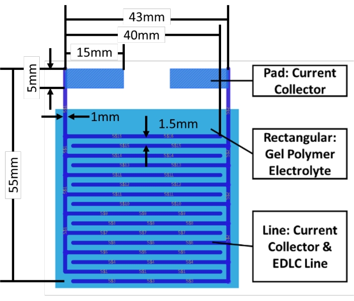
Figure 1: Interdigitated pattern designed with CAD program. The two pads at the top of the pattern are printed only with a current collector ink. The large sky-blue square is printed with a gel polymer electrolyte ink, and the blue lines are printed with the EDLC line ink and current collector ink. Please click here to view a larger version of this figure.

Figure 2: Image of the printer program window. (A) The first screen of the program. The red arrow shows where the Print button is. (B) The second screen of the program. The red arrow shows where the Simple button is. (C) The third screen of the program. Red arrow shows which ink should be selected. Please click here to view a larger version of this figure.
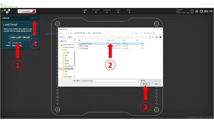
Figure 3: A screenshot showing how to upload the Gerber file of the designed pattern. Please click here to view a larger version of this figure.
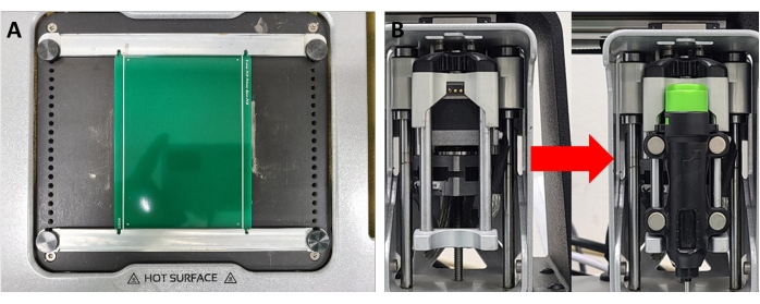
Figure 4: A screenshot showing how to fix the PCB board and mount the probe. (A) A top-view image of the inkjet printer which holds the PCB board. (B) The front-view image of the inkjet printer where the probe is mounted. Please click here to view a larger version of this figure.
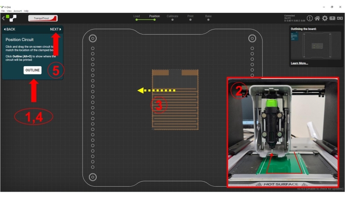
Figure 5: A screenshot showing how to check the probe movement when the pattern position is changed. Please click here to view a larger version of this figure.
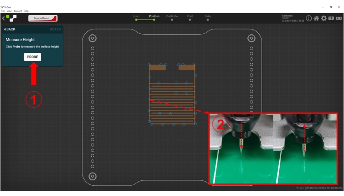
Figure 6: A screenshot showing how to measure surface height. After clicking on PROBE, the probe goes to the indicated spot on the substrate (denoted by circles), and then moves down and up to check the height of the substrate. Please click here to view a larger version of this figure.

Figure 7: A screenshot showing how to adjust the software parameters and print the sample pattern. (A) A screenshot image showing the procedure for printing a sample pattern. The red arrow indicates the button to print the sample pattern and the yellow arrow indicates the button to control the software parameters for the inks. (B) A window that appears when the yellow arrow shown in (A) is pressed. Software parameters can be modified by changing the values indicated by the 1 arrow. Press the 2 arrow to save the changes in software parameters. Please click here to view a larger version of this figure.
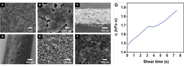
Figure 8: SEM image of the inks and printed layers, and EDLC ink viscosity. (A,B) Top-view SEM images of the current collector at (A) low magnification and (B) high magnification. (C) Tilted side-view SEM image of the printed EDLC active layer film. (D–F) Top-view SEM images of the EDLC active layer with different magnifications. (G) Apparent viscosity of EDLC ink versus shear time for constant 0.3 s-1 shear rate experiment. Adapted with permission from reference18. Copyright (2020) American Chemical Society. Please click here to view a larger version of this figure.
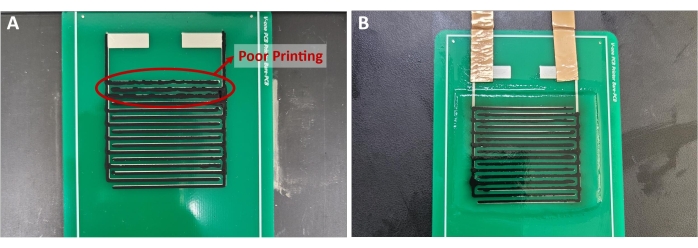
Figure 9: Photograph of the printed results. (A) Printing failure photo; the red circled part is printed unevenly due to printing failure. (B) Photograph of the final printed product. Please click here to view a larger version of this figure.
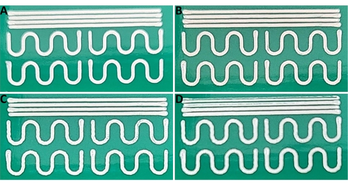
Figure 10: Printing results corresponding to the change in the feed rate. (A) 100 mm/min, (B) 300 mm/min, (C) 500 mm/min, and (D) 600 mm/min. Please click here to view a larger version of this figure.
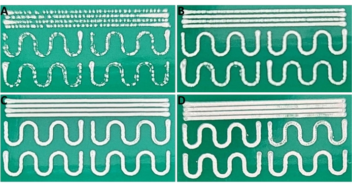
Figure 11: Printing results corresponding to the changes in the kick. (A) 0.1 mm, (B) 0.2 mm, (C) 0.35 mm, and (D) 0.7 mm. Please click here to view a larger version of this figure.

Figure 12: Printing results corresponding to the changes in the trim length. (A) 1.0 mm and (B) 50 mm. Please click here to view a larger version of this figure.
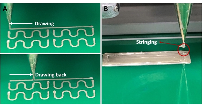
Figure 13: The pictures showing how the dispenser moves by the adjustment of the anti-stringing distance parameter. (A) Movement of the nozzle when the anti-stringing distance value is fixed at the maximum value (5.0 mm). (B) Photograph of stringing. Please click here to view a larger version of this figure.

Figure 14: Printing results corresponding to the change in the rheological setpoint change. (A) 0 and (B) 1.0. Red circles in (B) show the cracks (or holes) caused by the clogging effect. Please click here to view a larger version of this figure.

Figure 15: Printing results corresponding to the change in the soft start/soft stop ratio. The clockwise rotation of the sawtooth (red arrow) indicates the start of the printing. (A) Soft start maximum value and soft stop minimum value, as well as (B) soft start minimum value and soft stop maximum value. Please click here to view a larger version of this figure.

Figure 16: The electrochemical test results of the printed supercapacitor. (A) CV, (B) GCD, and (C) EIS graphs. Please click here to view a larger version of this figure.
| Parameter | Conductive ink | EDLC ink | GPE ink |
| Pass spacing (mm) | 0.15 | 0.15 | 0.15 |
| Dispense height (mm) | 0.12 | 0.14 | 0.16 |
| Feedrate (mm/min) | 500 | 300 | 300 |
| Trim length (mm) | 120 | 120 | 120 |
| Trace penetration (mm) | 0.15 | 0.15 | 0.15 |
| Anti-stringing distance (mm) | 0.4 | 0.7 | 0.1 |
| Kick (mm) | 0.35 | 0.3 | 0.4 |
| Soft start ratio | 0.1 | 0.8 | 0.8 |
| Soft stop ratio | 0.15 | 0.1 | 0.15 |
| Rheological setpoint | 0.16 | 0.2 | 0.16 |
Table 1. The optimized software parameters for conductive ink, EDLC ink, and GPE ink.
Discussion
The critical steps in this protocol are involved in the software parameter setup to print the designed pattern by finely adjusting the parameter values. Customized printing can lead to structural optimization and obtaining new mechanical properties19. The inkjet printing method with software parameter control can be used for sophisticated printing in various industries by selecting the optimized material for the printing process.
In the fabrication of supercapacitors using inkjet printing, one paper reported that there is still a limit to developing a pattern with uniform and high resolution. It has been reported that high-temperature post-treatment is still necessary, and the optimization process of the material is indispensable20. Another paper reported that to use inkjet printing properly, it is necessary to adjust the viscosity and surface tension in a relatively narrow range that depends on the printer. For this purpose, the concentration of the active material of the ink is limited. In some cases, it has been noted that multiple prints are necessary to deposit a sufficient amount of material21. In line with this trend, this protocol can help researchers implement patterns with higher resolution by providing precise methods for handling inkjet printers. In addition, with mastery over software control, one can simplify the manufacturing process by adjusting the software parameters such as Feed rate and Kick without having to print several times to deposit enough material.
Software parameter control for precise printing can be done according to the presented protocol. However, some bottlenecks should be addressed to improve the performance of the device based on the printing method.Various problems, such as ink spreading and clogging effect, require the optimization of the characteristics of the ink itself along with adjusting of software parameter values22. The two most crucial properties of the ink are viscosity and surface tension23. Therefore, the viscosity24 and surface tension25 of the ink must be measured and controlled for its optimization. To improve the performance, it is also important to fully understand the properties of the inks and to select materials with appropriate ratios.
In summary, a protocol is established here to use inkjet printing for printing a supercapacitor device. A discussion of software parameters controlling the inkjet printer has been provided here as a useful guide for handling and optimizing sophisticated printing processes. Further progress in printing wearable devices for energy storage, flexible sensors, and the aerospace industry can be achieved through ink material optimization.
Divulgations
The authors have nothing to disclose.
Acknowledgements
This work was supported by the Korea Electric Power Corporation (Grant number: R21XO01-24), the Competency Development Program for Industry Specialists of the Korean MOTIE operated by KIAT (No. P0012453), and the Chung-Ang University Graduate Research Scholarship 2021.
Materials
| 2” x 3” FR4 board | Voltera | SKU: 1000066 | PCB substrate |
| Activated carbon | MTI | Np-Ag-0530HT | |
| Eagle CAD | Autodesk | PCB CAD program | |
| Ethyl cellulose | Sigma Aldrich | 46070 | 48.0-49.5% (w/w) ethoxyl basis |
| Flex 2 conductive ink | Voltera | SKU: 1000333 | Flexible Ag ink |
| Lithium perchlorate | Sigma Aldrich | 634565 | |
| Propylene carbonate | Sigma Aldrich | 310328 | |
| PVDF | Sigma Aldrich | 182702 | average Mw ~534,000 by GPC |
| Smart Manager | ZIVE LAB | ver : 6. 6. 8. 9 | Electrochemical analysis program |
| Super-P | Hyundai | ||
| Terpineol | Sigma Aldrich | 432628 | |
| Thinky mixer | Thinky | ARE-310 | Planetary mixer |
| Triton-X | Sigma Aldrich | X100 | |
| V-One printer | Voltera | SKU: 1000329 | PCB printer |
| ZIVE SP1 | Wonatech | Potentiostat device |
References
- Valentine, A. D., et al. Hybrid 3D printing of soft electronics. Advanced Materials. 29 (40), 1703817 (2017).
- Liang, K., Carmone, S., Brambilla, D., Leroux, J. -. C. 3D printing of a wearable personalized oral delivery device: A first-in-human study. Science Advances. 4 (5), (2018).
- Joshi, S. C., Sheikh, A. A. 3D printing in aerospace and its long-term sustainability. Virtual and Physical Prototyping. 10 (4), 175-185 (2015).
- Wang, S., et al. Paper-based chemiluminescence ELISA: Lab-on-paper based on chitosan modified paper device and wax-screen-printing. Biosensors and Bioelectronics. 31 (1), 212-218 (2012).
- Vohra, V., et al. Low-cost and green fabrication of polymer electronic devices by push-coating of the polymer active layers. ACS Applied Materials & Interfaces. 9 (30), 25434-25444 (2017).
- Schüffelgen, P., et al. Selective area growth and stencil lithography for in situ fabricated quantum devices. Nature Nanotechnology. 14 (9), 825-831 (2019).
- Karim, N., Afroj, S., Tan, S., Novoselov, K. S., Yeates, S. G. All inkjet-printed graphene-silver composite ink on textiles for highly conductive wearable electronics applications. Scientific Reports. 9 (1), 8035 (2019).
- Singh, M., Haverinen, H. M., Dhagat, P., Jabbour, G. E. Inkjet printing-Process and its applications. Advanced Materials. 22 (6), 673-685 (2010).
- An, B., et al. Three-dimensional multi-recognition flexible wearable sensor via graphene aerogel printing. Chemical Communications. 52 (73), 10948-10951 (2016).
- Ko, S. H., Chung, J., Hotz, N., Nam, K. H., Grigoropoulos, C. P. Metal nanoparticle direct inkjet printing for low-temperature 3D micro metal structure fabrication. Journal of Micromechanics and Microengineering. 20 (12), 125010 (2010).
- Li, J., et al. Efficient inkjet printing of graphene. Advanced Materials. 25 (29), 3985-3992 (2013).
- Burke, A. Ultracapacitors: why, how, where is the technology. Journal of Power Sources. 91 (1), 37-50 (2000).
- Qorbani, M., Khajehdehi, O., Sabbah, A., Naseri, N. Ti-rich TiO2 tubular nanolettuces by electrochemical anodization for all-solid-state high-rate supercapacitor devices. ChemSusChem. 12 (17), 4064-4073 (2019).
- Areir, M., Xu, Y., Harrison, D., Fyson, J. 3D printing of highly flexible supercapacitor designed for wearable energy storage. Materials Science and Engineering: B. 226, 29-38 (2017).
- Fialkov, A. S. Carbon application in chemical power sources. Russian Journal of Electrochemistry. 36 (4), 345-366 (2000).
- Pandolfo, A. G., Hollenkamp, A. F. Carbon properties and their role in supercapacitors. Journal of Power Sources. 157 (1), 11-27 (2006).
- Egorov, V., Gulzar, U., Zhang, Y., Breen, S., O’Dwyer, C. Evolution of 3D printing methods and materials for electrochemical energy storage. Advanced Materials. 32 (29), 2000556 (2020).
- Seol, M. -. L., et al. All-printed in-plane supercapacitors by sequential additive manufacturing process. ACS Applied Energy Materials. 3 (5), 4965-4973 (2020).
- Park, S. H., Kaur, M., Yun, D., Kim, W. S. Hierarchically designed electron paths in 3D printed energy storage devices. Langmuir. 34 (37), 10897-10904 (2018).
- Sajedi-Moghaddam, A., Rahmanian, E., Naseri, N. Inkjet-printing technology for supercapacitor application: Current state and perspectives. ACS Applied Materials & Interfaces. 12 (31), 34487-34504 (2020).
- Komuro, N., Takaki, S., Suzuki, K., Citterio, D. Inkjet printed (bio)chemical sensing devices. Analytical and Bioanalytical Chemistry. 405 (17), 5785-5805 (2013).
- Kim, J., Kumar, R., Bandodkar, A. J., Wang, J. Advanced materials for printed wearable electrochemical devices: A review. Advanced Electronic Materials. 3 (1), 1600260 (2017).
- Calvert, P. Inkjet printing for materials and devices. Chemistry of Materials. 13 (10), 3299-3305 (2001).
- Zhou, Z., et al. High-throughput characterization of fluid properties to predict droplet ejection for three-dimensional inkjet printing formulations. Additive Manufacturing. 29, 100792 (2019).
- Ebnesajjad, S., Ebnesajjad, S. . Handbook of Adhesives and Surface Preparation. , 21-30 (2011).

