In Depth Analyses of LEDs by a Combination of X-ray Computed Tomography (CT) and Light Microscopy (LM) Correlated with Scanning Electron Microscopy (SEM)
Summary
A workflow for comprehensive micro-characterization of active optical devices is outlined. It contains structural as well as functional investigations by means of CT, LM and SEM. The method is demonstrated for a white LED which can be still be operated during characterization.
Abstract
In failure analysis, device characterization and reverse engineering of light emitting diodes (LEDs), and similar electronic components of micro-characterization, plays an important role. Commonly, different techniques like X-ray computed tomography (CT), light microscopy (LM) and scanning electron microscopy (SEM) are used separately. Similarly, the results have to be treated for each technique independently. Here a comprehensive study is shown which demonstrates the potentials leveraged by linking CT, LM and SEM. In depth characterization is performed on a white emitting LED, which can be operated throughout all characterization steps. Major advantages are: planned preparation of defined cross sections, correlation of optical properties to structural and compositional information, as well as reliable identification of different functional regions. This results from the breadth of information available from identical regions of interest (ROIs): polarization contrast, bright and dark-field LM images, as well as optical images of the LED cross section in operation. This is supplemented by SEM imaging techniques and micro-analysis using energy dispersive X-ray spectroscopy.
Introduction
This article demonstrates the potential and advantages of a combination of X-ray computed tomography (CT) with correlative light and electron microscopy (CLEM) for the exemplary in depth characterization of light emitting diodes (LED). With this technique it is possible to plan the micro preparation of the LED in such a fashion that while a cross section can be imaged microscopically the electrical functionality is preserved in the remainder of the specimen. The procedure has several unique features: firstly, the planned micro preparation by aid of the rendered volume of the entire sample obtained by CT; secondly, the observation of the LED by light microscopy (LM) with the complete variety of imaging techniques available (bright and dark field, polarization contrast, etc.); thirdly, observation of the LED in operation by LM; fourthly, observation of identical regions with the full variety of electron microscopy imaging techniques comprising secondary electron (SE) and back scatter electron (BSE) imaging, as well as energy dispersive X-ray fluorescence spectroscopy (EDX).
LEDs for illumination applications are designed to emit white light, although in certain applications color variability may be favorable. This broad emission cannot be achieved by emission from one compound semiconductor, since LEDs emit radiation in a narrow spectral band (circa 30 nm full width half maximum (FWHM)). Therefore white LED light is commonly generated by the combination a blue LED with phosphors which convert the short-wavelength radiation into broad emission over a large spectral range1. Color variable LED solutions usually make use of at least three primaries, which generally results in higher market prices.2
The use of either CT, LM or SEM is of course well established (e.g., in failure analysis for LEDs3–15), however the comprehensive and purposeful combination of all three techniques described here may offer new insights and will enable faster tracks towards meaningful characterization results.
From 3D microstructural analysis of the packaged device in CT the regions of interest (ROIs) can be identified and selected. With this non-destructive method, electrical connections can also be identified and considered for further preparation. The precise preparation of a 2D cross section allows investigations of the device in operation despite the destructive nature of this method. The cross section can now be characterized by CLEM16,17 which enables a very efficient and flexible characterization of identical ROIs with LM as well as SEM. By this approach, the advantages of both microscopy techniques can be combined. For example, a fast identification of ROIs in the LM is followed by high-resolution imaging in the SEM. But furthermore, the correlation of information from the LM (e.g., color, optical properties, particle distribution) with the visualization and analysis techniques of the SEM (e.g., particle size, surface morphology, element distribution) allows a deeper understanding of functional behavior and microstructure within a white LED.
Protocol
1. Sample Preparation for X-ray Computed Tomography (CT)
- Glue sample (LED cf. materials section) to a 2 mm Ø hollow carbon fiber bar of appropriate length using hot-melt adhesive.
- Adjust position of specimen by using a hot-air gun if needed. Fix the sample in the CT-sample chamber using the three-jaw chuck.
2. CT Measurement Setup
- Perform warmup and centering procedures according to the control software of the X-ray tube.
NOTE: Use tube-control software of manufacturers' CT and standard protocol as specified by the supplier (cf. materials section). - Calibrate beam and detector using data acquisition software, such as that specified in the materials section. Determine dark current and adjust offset and gain of the detector according to the standard procedures provided by the manufacturer (cf. materials section).
- Adjust imaging parameters. For the results shown here, use the following adjustments: Set image magnification to 36.37, set Voxel Size to 1.37 µm, set number of images to 1,800 (per 360°), set imaging time to 500 msec, set number of averaged images to 3 and number of skipped frames to 1, set image size to 2,284 x 2,304 pixel.
- Adjust measurement parameters. For the results shown use the following adjustments: Set focus object distance (FOD) to 5.5 mm, set focus detector distance (FDD) to 200 mm, set X-ray tube voltage to 100 kV and tube current to 135 µA, use 0.2 mm Cu foil for beam hardening.
3. Performance of CT Scan
NOTE: X-ray intensities may vary during the measurement. To compensate for these eventual fluctuations, a region of interest (ROI) window is placed where the X-rays will not interfere with the sample. This region is not affected by X-ray absorption through the sample, it is therefore the region with the highest measured intensity.
- Select the ROI by identifying the area not obscured by the measured object during one full rotation. In the measurement window with the live image, press and hold the left mouse button and draw up a red framed window.
- Right click on this window's frame to open a context menu. Then select "set as observation window". The frame's color will change to yellow, and the observation window will be fixed in the measurement window.
NOTE: Using this software function therefore sets the observation window and defines the region in the scanned-images, where the X-rays do not interact with the sample. This is to correct for possible drift of gray-values for rays, which directly hit the detector (free rays, causing the gray-value of air). It is the brightest region in the image during a full rotation of the sample.
NOTE: Due to the fact that heating of the X-ray tube will lead to thermal expansions of tube materials, a software module is activated which corrects for such effects. These effects cause shifts in the X-ray foci on the target as well as spatially, which during the measurement will cause a movement of the measured object in the recorded images.- Activate the software module "auto scan optimizer", through which nine images are taken before the actual scan of the sample. These images are taken in 40° steps, while rotating the sample.
NOTE: This software module will in addition to the correction of thermal effects also allow for the correction of smaller mechanical movements of the sample itself. The module is found in the graphical user interface of the measurement software. - Additionally activate the module "detector shift routine". The simultaneous activation of these two modules before starting the actual CT scan ensures correction for movements of the sample and for ring artifacts.
NOTE: This software module is used to reduce ring artifacts: The detector is moved to a position ca. ±10 pixels from the initial position and all images taken are averaged. This reduces the influence faulty pixels. - Use the "auto scan optimizer" and "detector shift routine" of the acquisition software for the purpose described above, the two modules are selected separately and are used simultaneously in this investigation.
- Activate the software module "auto scan optimizer", through which nine images are taken before the actual scan of the sample. These images are taken in 40° steps, while rotating the sample.
- Scan sample by starting the "data acquisition routine" in the acquisition software.
4. Reconstruction of Volume Information, Planning of Micro Preparation
- Use manufacturers' reconstruction software to render volume information. Volume rendering is carried out digitally using a computing cluster to reconstruct the sample features presented by X-ray absorption.
- Apply image correction algorithms: bhc+ (beam hardening correction) applying the value for "different materials" (which is 5.8) to remove beam hardening and scan optimizer to remove unwanted sample movements cf. 3.2). Carry these steps out according to the supplier's software manual (cf. materials section).
- Choose an area for reconstruction, and define a region of interest (ROI). In this case the ROI is defined by the volume the LED occupies during a full circle described by its rotation in the CT sample chamber. Make use of the software options "use observation" and "ROI CT-filter" to suppress artifacts, stick to the supplier's software manual (cf. materials section), when doing this.
- Reconstruct the volume for ROI. After setting ROI, filters and correction options in the reconstruction software, carry out the volume reconstruction using the computing cluster as specified by the instrument's supplier (cf. materials section).
- Transfer reconstruction data to the CT-data-analysis software, align sample in xy, xz and yz planes using the "simple registration" function in the software. Apply "median" filtering, using filter size "3".
NOTE: Carry the following steps out as described in the software manual (cf. materials section).- Using the software, inspect the rendered volume, and check for the electrical interconnects in the device structure to ensure supply of electrical current from the soldering pads underneath the device to the light emitting semiconductor chip on top.
- Define cutting position and amount of sample to be removed by grinding and polishing for the subsequent micro preparation, such that after removal the device is still operational (avoid open circuitry). Use distance and measurement tools of the software to ensure operability of the specimen after micro preparation (length may be calibrated by the known LED-chip dimensions of 1 mm x 1 mm).
5. Micro Preparation
- Solder silver wire to the anode and cathode pads of the LED manually. Use solder wire of 1 mm diameter and with the composition 60% Sn, 39% Pb and 1% Cu. Ensure appropriate positioning of the wires.
- Embed LED in epoxy-resin using transparent supports (e.g., rings of 25 mm or 40 mm diameter). Drill two small holes on opposite sides of the support and feed the silver wire (which contacts the LED) through it. Position LED by means of tightening or loosening the silver wire to align the front edge of the LED and the support.
- Fill the ring with epoxy inside a silicone beaker pretreated to ensure that it will not stick to the epoxy and subsequently let the epoxy harden.
- Using a stereomicroscope, visually ensure that support and LED are aligned. Mechanically remove any resin, which is in excess (e.g., outside of the support), by grinding with coarse abrasive paper.
- Fix the LED (embedded in the epoxy resin), in a planar fashion to a sample holder , for precision grinding.
- Use a grinder with abrasion measurement and remove the sample surface up to 100 µm from the targeted plane's position.
- Carefully remove further material on a manually operated grinder using 9 µm diamond suspension. Control the progress in abrasion frequently with a stereo microscope.
- On reaching the targeted region, as defined by the CT scan, switch to 3 µm diamond suspension and finally suitable polishing suspensions, by changing to the corresponding grinding and polishing discs of the manual grinder used. Control the progress in short intervals with a stereo microscope.
NOTE: Ideally the prepared surface will now correspond to the target plane defined in the CT measurement. - In steps 5.5 and 5.6 always remove grinding and polishing suspensions before using the microscope by rinsing with de-ionized water and wiping with cotton pads.
- After polishing, observe the smooth and scratch free surface using a stereo microscope. Clean the specimen with de-ionized water and cotton pads, and remove water by rinsing with ethanol (pure methylated spirit) and drying using a hair dryer.
- Check the specimen for electrical operability, i.e., current flow through the light emitting diode in forward direction and no current flow in reverse direction, using a digital multimeter.
6. LM Measurement Setup
- Mount specimen in appropriate sample holder for CLEM (cf. materials section). Ensure that the sample holder fixes the sample for use in LM, Sputter Coater and SEM.
- Adjust calibration marks (L-structures on the holder) to the same height as sample surface (ca. 4 mm). Ensure that the polished surface is parallel to focal plane of the LM. Fix sample holder onto the motorized xy-stage of LM. Connect LED to power supply. The power supply should operate in constant current mode.
- Calibrate sample holder position on the xy-stage by saving the position of calibration marks as reference points.
NOTE: A detailed instruction for this step including semi-automatic procedure is described in the user manual (cf. materials section).
7. LM Characterization
- Move xy-stage of LM such that ROI of the sample is in the field of view of the LM. Ensure that the LM camera has an accurate white balance by auto-calibration as provided in the LM-software and use of a white reference surface (e.g., sheet of paper).
- Perform LM imaging in a compound LM with reflected light according to the steps described in the user manual provided by the supplier (cf. materials section). For the results shown here the bright field, dark field, and polarization contrast were imaged with a 50X objective.
- Switch on the power supply and tune LED emission. Switch off LM illumination and adjust exposure time of the LM camera (ca. 92 msec dependent on emission intensity). Obtain LM image of light distribution within the sample (Luminescence contrast).
- If applicable, image luminescence together with other contrasts by activating LM illumination and LED simultaneously.
NOTE: Otherwise, images with different contrasts can also be mixed by means of image processing later on. - Save all LM images together with the corresponding stage position as described in the user manual provided by the supplier (cf. materials section).
8. Sputter Coating
- Remove sample holder from LM and power supply. Make sure that the sample remains stably fixed within the holder.
- Fix Copper conductive tape onto the polished sample surface around the LED and contacting the sample holder. Do not cover the ROIs with the tape.
- Using a foil cover the sample holder and prepare a window similar to the sample diameter (ca. 5 mm). Fix the complete sample holder within the foil such that the window is directly above the sample.
- Place the sample holder into the recipient of the sputter coater ensuring that the sample surface can be coated. Sputter a 5 nm thick carbon layer onto the sample surface (from carbon rod). Move the sample holder out of the sputter coater and remove the foil.
9. SEM Measurement Setup
- Mount sample holder onto the SEM adapter and place it on the motorized stage of SEM. Pump the vacuum chamber.
- Calibrate sample holder position within the SEM by saving the position of calibration marks as reference points.
NOTE: A detailed instruction for this step including semi-automatic procedure is described in the user manual (cf. materials section). - Define coordinate transformation from LM to SEM stage for direct relocation of ROIs and for navigation within the LM images. This step can also be done automatically by software as described in the user manual (cf. materials section).
10. SEM Analysis
- Move stage to show ROI on sample and perform SEM analysis in the same location as in the LM.
- Select "SE detection" for surface imaging. Choose electron energy of 20 keV, set the aperture to 30 µm and position the sample at a working distance of 8.7 mm.
- Select "BSE detection" for material contrast. Choose electron energy of 20 keV, set the aperture to 30 µm and position the sample at a working distance of 8.7 mm.
- Select "EDX detection" for element mapping. Choose electron energy of 20 keV, set the aperture to 60 µm and position the sample at a working distance of 9 mm. Detect the following elements: Y, Al, Ca, Si, Ga, Au, Ni, and Cu.
11. Image Processing
- Perform overlay of LM and SEM images by selecting identical points in the images from LM and SEM and by further image processing as described in the user manual provided by the supplier (cf. materials section).
Representative Results
The characterized LED is shown in Figure 1. It is a white emitting LED with a Chip size of 1 x 1 mm2 and a partially ceramic luminescent color converter. Gluing the LED in a slightly slanted position onto a carbon fiber bar avoids CT artifacts caused by sample symmetry (Figure 2). Results of the CT measurement allow for planning the position of the cross section of the sample, and ensure electrical operability after partial abrasion (Figure 3 and Figure 4). The rendered volume allows for the localization of functional structures, especially the electrical contacts that are easily distinguishable due to the high atomic numbers of the corresponding metals (Au, Cu, Sn), which lead to high contrast in the underlying X-ray images. If the basic architecture of the LED package is known, the volumes occupied by the active region (i.e., light emitting chip), phosphors, Zener diode and over-molded optics are easily identified. For further preparation, the sample is embedded in epoxy resin (Figure 5). Electrical contacts are provided to allow operation of the LED. Subsequently, the sample surface is removed and the cross section is polished according to the planning by CT. The cross section is imaged in the LM. Simultaneous brightfield illumination and LED emission (Figure 6) allow for the visualization of the blue emission from the LED chip and different phosphor materials, together with the structural setup of this device. Here the light spreading in the different functional layers, as well as the conversion of blue to red and yellow photons can be localized visually. The overlay of the brightfield contrast shows the position of Au contacts and packaging materials like Si.
After sputter coating of the sample surface and transferring the CLEM sample holder to SEM, the ROI is imaged with BSE contrast (Figure 7). Electron microscopy in correlation with LM allows the following deductions: The red emitting phosphor (high contrast) is embedded in a matrix (low contrast, probably silicone), which also functions as adhesive for the ceramic yellow emitting conversion layer on top. Particle sizes and morphologies in the conversion layers can easily be recognized, and the homogeneity of the distribution of the red emitting material can also be assessed. This analysis additionally gives an estimate of the relative quantities of the two phosphors.
Correlating the information of both methods (Figure 8) links the functional behavior to the microstructure of the device in an additional ROI. Here, finally, the deductions made in the previous steps as related to the nature of the materials identified can be confirmed. By quantitative EDS measurements, the exact constituents of this LED package can easily be identified: viz. InGaN active region, CaAlSiN3:Eu red emitting phosphor and Y3Al5O12:Ce yellow emitting ceramic phosphor.
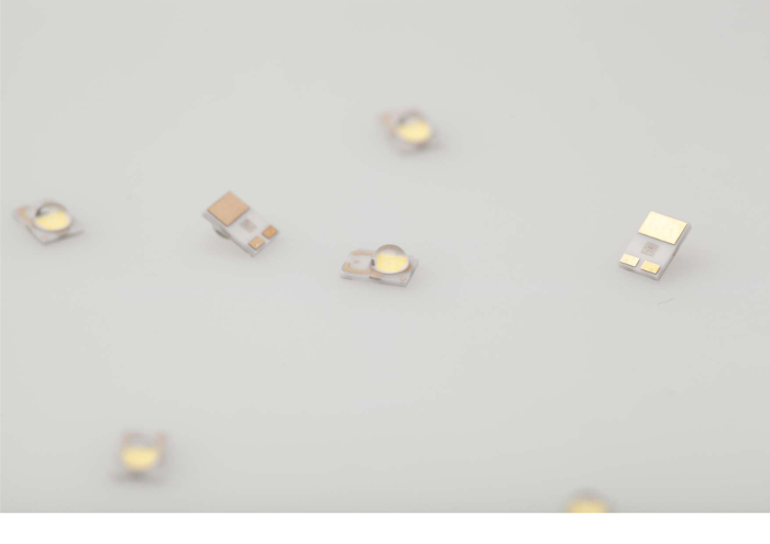
Figure 1. LED. LED used for characterization. Please click here to view a larger version of this figure.
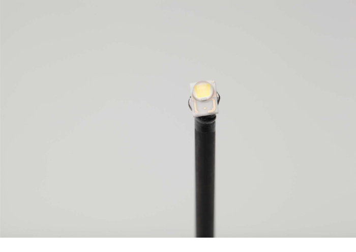
Figure 2. Specimen prepared for CT. LED mounted on carbon fiber bar in slanted position. Please click here to view a larger version of this figure.
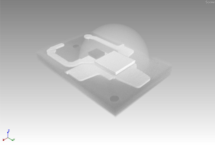
Figure 3. Rendered volume. Rendered volume as result of CT measurement. Scales may be estimated from the square ceramic phosphor platelet covering the light emitting chip, which is 1 mm x 1 mm in size. Please click here to view a larger version of this figure.
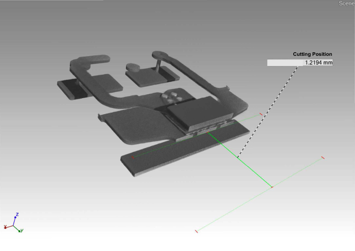
Figure 4. Planned cross section. Virtual planning of cross sections ensures electrical operability. Please click here to view a larger version of this figure.
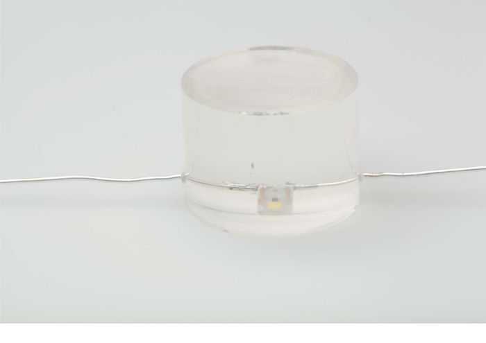
Figure 5. Embedded sample. Sample embedded in epoxy resin with electrical contact wires. Please click here to view a larger version of this figure.
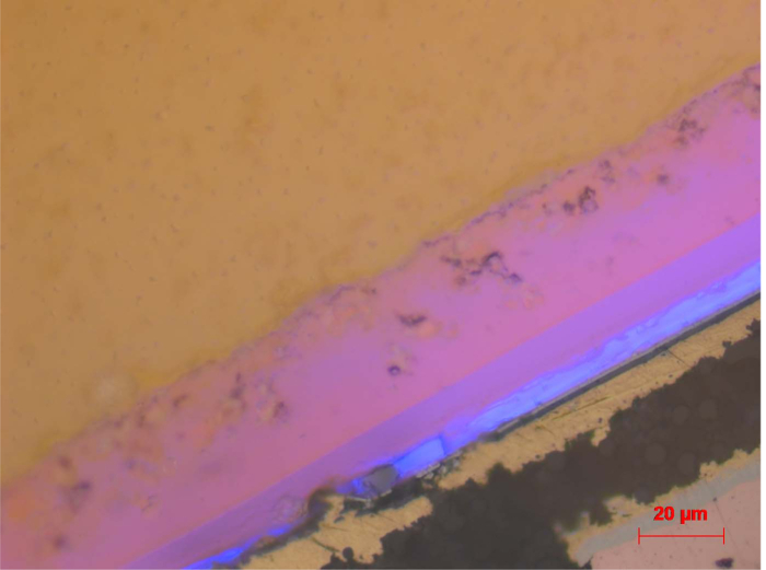
Figure 6. LM image of cross section. Cross section of lit up LED imaged with simultaneous bright field illumination. Scale bar is 20 µm. Please click here to view a larger version of this figure.
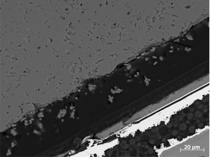
Figure 7. SEM image of cross section. BSE image of the same ROI as in Figure 6. Scale bar is 20 µm. Please click here to view a larger version of this figure.
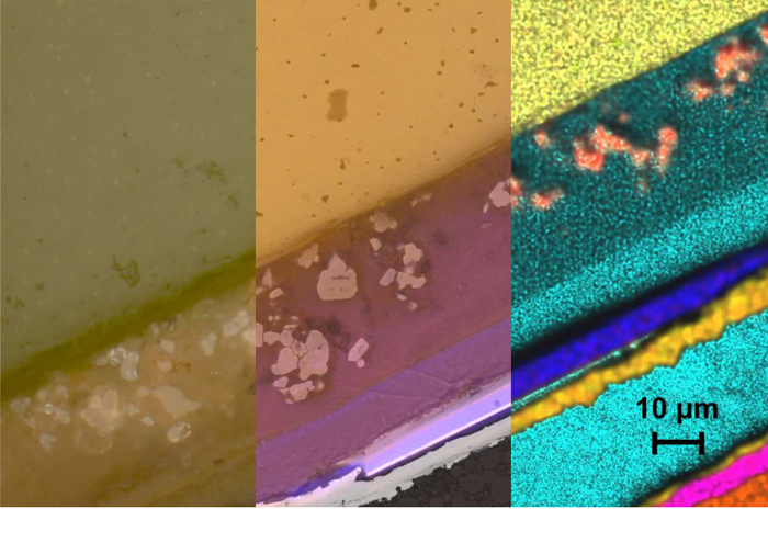
Figure 8. CLEM image of cross section. Overlay of LM and SEM images (from left to right): brightfield contrast in LM, Overlay of luminescence contrast (LM) and backscattered electrons (SEM) energy dispersive X-ray fluorescence mapping in SEM (Y light yellow, Al green, Ca red, Si turquoise, Ga blue, Au yellow, Ni pink, Cu brown). Scale bar is 10 µm. Please click here to view a larger version of this figure.
Discussion
The advantages of this multimodal approach consist in the location-dependent correlation of the acquired data. The multimodal approach described here should be contrasted in subsequent analyses with each technique separately. For example, luminescence properties visible in LM can be linked to compositions as detected using SEM/EDS. The volume information obtained by CT can be extended with in depth analyses of cross-sections prepared in a targeted fashion. CT data also enable fast location of possible areas of interest in the subsequent microscopic investigations. The method described here is finally one of the few techniques which enable the linkage of optical properties to the microstructure and even to sub micrometer structural details. Optical defects or inhomogeneities can definitively and traceably be linked to structural or electrical defects of the devices.
The method proposed here relies on excellent and reliable data obtained by each of the imaging techniques used. This is critical especially in view of the CT results which must be precise enough to obtain clear structural information in an area as small as 1 mm3 and well below. If the uncertainties are too large successful planning for the location of planes suited for cross sections leaving the device electronically intact will be impossible. However, not only does the correct placement of the cross section ensures electrical operability, but, in addition, during the grinding and polishing processes care has to be taken in order to avoid short-circuiting the device by mechanical stress or unwanted particles (e.g., from grinding media) introduced into the sample surface.
If the LED proves to be short circuited despite correct placement of the cutting plane and careful preparation, it may be useful to re-inspect the surface for particles which cause this electrical failure. Careful polishing of the sample surface is recommended for troubleshooting in such cases, usually operability of the device can be established by this measure. Further improvement of the sample surface is possible by the use of ion milling techniques. Thereby the area observed microscopically will be optimally smooth and defect free. Once cross sections have successfully been prepared the handling of the CLEM sample holder has to be carried out with utmost diligence. Small movements of the sample relative to the holder will make overlays imprecise and undermine the advantages of the technique due to the fact that in those cases ROIs will again have to be found manually.
This workflow is limited to samples which allow for sufficient contrast differences in CT imaging (X-ray absorption may neither be too high nor too low). Samples with small form factors are preferred. The aspect ratio of the sample has to be such that not too small amounts need to be removed for cross section preparation. In this example 1.2 mm were removed, if this distance is much smaller more precise grinding or polishing techniques need to be applied, e.g., ion milling. The diffraction limit of light microscopy resolution can partially be overcome for different types of contrast by subsequent SEM imaging of the ROI.
This technique may prove extremely useful in micro-characterization, failure analysis or reverse engineering of micro electronic devices. Due to the possibility to virtually plan the destructive parts of the sample analysis, more precise and planned preparations can be carried out reducing analysis time and failures.
In the future the extension of this technique towards laser diodes and further semiconductor light sources is planned. The CLEM technique would also allow for the implementation of fluorescence microscopy, which can enable in depth analysis of the light emitting materials present (e.g., excitation and emission spectra or luminescence lifetimes). Focused Ion Beam (FIB) instruments could be used to speed up sample preparation, in this case samples would be prepared using FIB and the CLEM workflow (position calibration) would start in the FIB. Another way of working using FIB would be to destructively determine the sample's 3D structure in a FIB-SEM.
The results shown here are of an exemplary nature illustrating the technique as such. It is obviously possible to use each of the mentioned techniques in a far more sophisticated fashion, therefore we also expect further insights from future experiments.
Offenlegungen
The authors have nothing to disclose.
Acknowledgements
The authors kindly acknowledge financial support from the "Akademische Gesellschaft Lippstadt" as well as from the "Ministerium für Innovation, Wissenschaft und Forschung des Landes Nordrhein-Westfalen". Photographs in Figures 1, 2 and 5 courtesy to Markus Horstmann, Hamm-Lippstadt University of Applied Sciences.
Materials
| X-Ray Computer Tomograph | General Electric | not applicable | type: nanotom s research edition |
| acquisition software | General Electric | not applicable | phoenix Datos| x2 acquisition and corresponding manual |
| reconstruction software | General Electric | not applicable | phoenix Datos| x2 acquisition and corresponding manual |
| rendering software | Volume Graphics | not applicable | VGStudio Max 2.2 and corresponding manual |
| grinder (manual) | Struers | 5296327 | Labopol 21 |
| sample holder | Struers | 4886102 | UniForce |
| grinder (automated) | Struers | 6026127 | Tegramin 25 |
| epoxy resin/hardener | Struers | 40200030/40200031 | Epoxy fix resin / Epoxy fix hardener |
| Ethanol | Struers | 950301 | Kleenol |
| Light Microscope | Zeiss | not applicable | Axio Imager M2m |
| Electron Microscope | Zeiss | not applicable | Sigma |
| CLEM software | Zeiss | not applicable | Axio Vision SE64 Rel.4.9 and corresponding manual |
| CLEM sample holder | Zeiss | 432335-9101-000 | Specimen holder CorrMic MAT Universal B |
| SEM Adapter for CLEM sample holder | Zeiss | 432335-9151-000 | SEM Adapter for Specimen holder CorrMic MAT Universal B |
| sputter coater | Quorum | not applicable | Q150TES |
| EDS detector | Röntec | not applicable | X-Flash 1106 |
| solder | Stannol | 535251 | type: HS10 |
| LED | Lumileds | not applicable | LUXEON Rebel warm white, research sample |
Referenzen
- Mueller-Mach, R., Mueller, G. O., Krames, M. R., Trottier, T. High-power phosphor-converted light-emitting diodes based on III-Nitrides. IEEE J. Sel. Top. Quantum Electron. 8 (2), 339-345 (2002).
- Branas, C., Azcondo, F. J., Alonso, J. M. Solid-State Lighting: A System Review. IEEE Ind. Electron. Mag. 7 (4), 6-14 (2013).
- Chang, M. -. H., Das, D., Varde, P. V., Pecht, M. Light emitting diodes reliability review. Microelectron. Reliab. 52 (5), 762-782 (2012).
- Ayodha, T., Han, H. S., Kim, J., Kim, S. Y. Effect of chip die bonding on thermal resistance of high power LEDs. Intersoc. Conf. Therm. Thermomechanical Phenom. Electron. Syst. ITHERM. , 957-961 (2012).
- Cason, M., Estrada, R. Application of X-ray MicroCT for non-destructive failure analysis and package construction characterization. Proc. Int. Symp. Phys. Fail. Anal. Integr. Circuits, IPFA. , (2011).
- Chen, R., Zhang, Q., Peng, T., Jiao, F., Liu, S. Failure analysis techniques for high power light emitting diodes. 2011 12th Int. Conf. Electron. Packag. Technol. High Density Packag. , 1-4 (2011).
- Chen, Z., Zhang, Q., et al. Study on the reliability of application-specific led package by thermal shock testing, failure analysis, and fluid-solid coupling thermo-mechanical simulation. IEEE Trans. Components, Packag. Manuf. Technol. 2 (7), 1135-1142 (2012).
- Luniak, M., Holtge, H., Brodmann, R., Wolter, K. -. J. Optical Characterization of Electronic Packages with Confocal Microscopy. 2006 1st Electron. Syst. Technol. Conf. 2 (16), 1813-1815 (2006).
- Marks, M. R., Hassan, Z., Cheong, K. Y. Characterization Methods for Ultrathin Wafer and Die Quality: A Review. IEEE Trans. Components, Packag. Manuf. Technol. 4 (12), 2042-2057 (2014).
- Rosc, J., Hammer, H., et al. Reliability assessment of contact wires in LED-devices using in situ X-ray computed tomography and thermo-mechanical simulations. Proc. 5th Electron. Syst. Technol. Conf. , 1-6 (2014).
- Zhaohui, C., Qin, Z., Kai, W., Xiaobing, L., Sheng, L. Reliability test and failure analysis of high power LED packages. J. Semicond. 32 (1), 014007 (2011).
- Hamon, B., Bataillou, B., Hamon, B., Mendizabal, L., Gasse, A., Feuillet, G. N-contacts degradation analysis of white flip chip LEDs during reliability tests. 2014 IEEE Int. Reliab. Phys. Symp. , FA.1.1-FA.1.6 (2014).
- Tsai, M. -. Y., Tang, C. -. Y., Yen, C. -. Y., Chang, L. -. B. Bump and Underfill Effects on Thermal Behaviors of Flip-Chip LED Packages: Measurement and Modeling. IEEE Trans. Device Mater. Reliab. 14 (1), 161-168 (2014).
- Wang, F. -. K., Lu, Y. -. C. Useful lifetime analysis for high-power white LEDs. Microelectron. Reliab. 54 (6-7), 1307-1315 (2014).
- Liu, Y., Zhao, J., Yuan, C. C. -. A., Zhang, G. Q., Sun, F. Chip-on-Flexible Packaging for High-Power Flip-Chip Light-Emitting Diode by AuSn and SAC Soldering. IEEE Trans. Components, Packag. Manuf. Technol. 4 (11), 1754-1759 (2014).
- Thomas, C., Edelmann, M., Lysenkov, D., Hafner, C., Bernthaler, T., Schneider, G. Correlative Light and Electron Microscopy (CLEM) for Characterization of Lithium Ion Battery Materials. Microsc. Microanal. 16, 784-785 (2010).
- Thomas, C., Ogbazghi, T. Correlative Microscopy of Optical Materials. Imaging & Microscopy. 3, 32-34 (2014).

